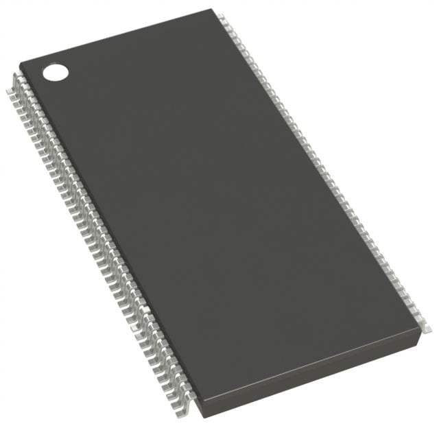
IS45S32400B-7TLA1
| Part Description |
IC DRAM 128MBIT PAR 86TSOP II |
|---|---|
| Quantity | 976 Available (as of June 9, 2026) |
| Product Category | Memory |
|---|---|
| Manufacturer | Integrated Silicon Solution Inc |
| Manufacturing Status | Obsolete |
| Manufacturer Standard Lead Time | Contact Us |
| Datasheet |
Specifications & Environmental
| Device Package | 86-TSOP II | Memory Format | DRAM | Technology | SDRAM | ||
|---|---|---|---|---|---|---|---|
| Memory Size | 128 Mbit | Access Time | 5.4 ns | Grade | Industrial | ||
| Clock Frequency | 143 MHz | Voltage | 3V ~ 3.6V | Memory Type | Volatile | ||
| Operating Temperature | -40°C ~ 85°C (TA) | Write Cycle Time Word Page | N/A | Packaging | 86-TFSOP (0.400", 10.16mm Width) | ||
| Mounting Method | Volatile | Memory Interface | Parallel | Memory Organization | 4M x 32 | ||
| Moisture Sensitivity Level | 3 (168 Hours) | RoHS Compliance | ROHS3 Compliant | REACH Compliance | REACH Unaffected | ||
| Qualification | N/A | ECCN | EAR99 | HTS Code | 8542.32.0002 |
Overview of IS45S32400B-7TLA1 – IC DRAM 128MBIT PAR 86TSOP II
The IS45S32400B-7TLA1 is a 128 Mbit synchronous DRAM organized as 4M × 32 with a parallel memory interface and fully synchronous, clocked operation. It implements a quad-bank architecture and pipeline operation for high-rate burst transfers and internal bank interleaving.
Designed for systems requiring a 128 Mbit SDRAM device in an 86‑pin TSOP II footprint, the device supports programmable burst lengths and CAS latencies, built‑in refresh modes and self‑refresh to maintain data integrity in active and low‑power states.
Key Features
- Memory Organization — 128 Mbit arranged as 4M × 32 with four internal banks to support concurrent bank operations and hidden precharge cycles.
- Synchronous SDRAM Core — Fully synchronous operation with all signals referenced to the rising clock edge and LVTTL-compatible inputs.
- Speed and Timing — Supports clock rates including 143 MHz (other options: 166, 125, 100 MHz) with access time as low as 5.4 ns (CAS latency = 3).
- Programmable Burst and CAS — Programmable burst lengths (1, 2, 4, 8, full page), sequential/interleave burst sequences and CAS latency options (2 or 3 clocks) for flexible performance tuning.
- Refresh and Power Modes — Auto Refresh (CBR), Self Refresh with programmable refresh periods and 4096 refresh cycles every 64 ms to preserve data across idle intervals.
- Voltage and Interface — Operates from 3.0 V to 3.6 V (nominal 3.3 V) with separate VDD/VDDQ supplies and a parallel LVTTL interface.
- Package and Temperature — 86‑pin TSOP II (0.400", 10.16 mm width) package; rated for operation from −40 °C to 85 °C (TA).
- Burst Read/Write Support — Burst read/write and burst read/single write capability with burst termination via burst stop and precharge command.
Typical Applications
- Synchronous memory subsystems — Provides 128 Mbit SDRAM capacity for systems that require a parallel, clocked DRAM interface and programmable burst behavior.
- Industrial equipment — Industrial temperature rating (−40 °C to 85 °C) suits embedded controllers and equipment operating across wide thermal ranges.
- Board-level replacements/retrofits — Standard 86‑TSOP II package fits designs using the TSOP II footprint where 128 Mbit SDRAM is required.
Unique Advantages
- Flexible performance scaling: Multiple clock-frequency grades (including 143 MHz) and CAS latency options allow tuning for throughput or timing compatibility.
- Banked architecture: Quad-bank internal organization enables bank interleaving to hide precharge time and improve effective random-access performance.
- Comprehensive refresh support: Auto and self-refresh modes with defined refresh cycles (4096 per 64 ms) simplify retention management for varied duty cycles.
- Industry-standard interface and package: LVTTL-compatible parallel interface and 86‑pin TSOP II packaging simplify integration into existing board designs.
- Wide operating range: 3.0–3.6 V supply window and −40 °C to 85 °C operating temperature provide design margin for harsh environments.
- Configurable burst behavior: Programmable burst lengths and sequences allow optimization for sequential or random access patterns.
Why Choose IS45S32400B-7TLA1?
The IS45S32400B-7TLA1 combines a synchronous, pipeline SDRAM architecture with configurable burst and timing options to deliver a flexible 128 Mbit memory building block. Its quad-bank organization, refresh features and LVTTL interface make it suitable for designs that need predictable, clocked memory behavior in an 86‑pin TSOP II package.
This device is appropriate for engineers specifying a robust SDRAM component for board-level designs that require programmable latency, burst options and industrial temperature operation. Its standard footprint and voltage range support integration into existing layouts while providing scalability across multiple frequency grades.
Request a quote or contact the sales team to discuss availability, lead times and volume pricing for the IS45S32400B-7TLA1.