IS45S32400E-6TLA1
| Part Description |
IC DRAM 128MBIT PAR 86TSOP II |
|---|---|
| Quantity | 1,087 Available (as of June 15, 2026) |

| Product Category | Memory |
|---|---|
| Manufacturer | Integrated Silicon Solution Inc |
| Manufacturing Status | Obsolete |
| Manufacturer Standard Lead Time | Contact Us |
| Datasheet |
Specifications & Environmental
| Device Package | 86-TSOP II | Memory Format | DRAM | Technology | SDRAM | ||
|---|---|---|---|---|---|---|---|
| Memory Size | 128 Mbit | Access Time | 5.4 ns | Grade | Industrial | ||
| Clock Frequency | 166 MHz | Voltage | 3V ~ 3.6V | Memory Type | Volatile | ||
| Operating Temperature | -40°C ~ 85°C (TA) | Write Cycle Time Word Page | N/A | Packaging | 86-TFSOP (0.400", 10.16mm Width) | ||
| Mounting Method | Volatile | Memory Interface | Parallel | Memory Organization | 4M x 32 | ||
| Moisture Sensitivity Level | 3 (168 Hours) | RoHS Compliance | ROHS Compliant | REACH Compliance | REACH Unaffected | ||
| Qualification | N/A | ECCN | EAR99 | HTS Code | 8542.32.0002 |
Overview of IS45S32400E-6TLA1 – IC DRAM 128MBIT PAR 86TSOP II
The IS45S32400E-6TLA1 is a 128Mbit synchronous DRAM organized as 4M × 32 with a parallel interface and quad-bank internal architecture. It uses a pipelined, fully synchronous design to support high-speed data transfer in 3.3V memory systems.
Designed for systems requiring a compact board-level DRAM, the device offers programmable burst modes, selectable CAS latency, and standard 86-pin TSOP-II packaging to simplify integration into parallel memory subsystems operating across commercial and industrial temperature ranges.
Key Features
- Core / Architecture Quad-bank synchronous DRAM internally organized as 1M × 32 × 4 banks for parallel access and bank-overlap operations.
- Memory Capacity & Organization 128 Mbit total capacity arranged as 4M × 32, suitable for 32-bit wide memory buses.
- Performance & Timing Clock frequency up to 166 MHz (−6 speed grade) with programmable CAS latency (2 or 3 clocks) and access time as low as 5.4 ns for CL=3.
- Burst & Access Modes Programmable burst length (1, 2, 4, 8, full page) and selectable burst sequence (sequential or interleave) with burst read/write and burst read/single write support.
- Refresh & Self-Maintenance Auto refresh (CBR) and self-refresh supported; refresh rates of 4096 cycles per 16 ms (A2) or 64 ms (commercial/industrial/A1 options) as specified.
- Interface & Signaling LVTTL-compatible parallel interface with all signals referenced to the positive clock edge for fully synchronous operation.
- Power Single power supply operation at 3.0 V to 3.6 V (3.3 V ±0.3 V specified in the datasheet).
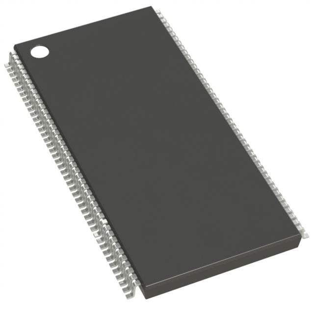
- Package & Temperature Available in an 86-pin TSOP-II (86-TFSOP, 0.400" / 10.16 mm width) and rated for operating temperatures down to −40°C up to +85°C (industrial grade).
Typical Applications
- 3.3 V Memory Subsystems Acts as board-level SDRAM in systems designed for a 3.3 V memory supply.
- Parallel Bus Designs Provides 32-bit wide, parallel DRAM storage for designs requiring 4M × 32 organization and burst-access capability.
- Industrial Temperature Systems Suitable for equipment operating across commercial and industrial ambient ranges (−40°C to +85°C).
Unique Advantages
- Flexible Burst Control: Programmable burst lengths and sequence options let designers optimize throughput and latency for varied access patterns.
- Selectable CAS Latency: CAS latency options (2 or 3 clocks) enable tuning of access timing to match system clocking and performance targets.
- High-Speed Synchronous Operation: Up to 166 MHz clocking with pipeline architecture supports rapid, predictable data transfer referenced to the clock edge.
- Integrated Refresh Support: Built-in auto refresh and self-refresh mechanisms simplify system refresh management and maintain data integrity.
- Industry-Grade Temperature Range: Specified operation from −40°C to +85°C to meet harsher ambient requirements.
- Standard TSOP-II Packaging: 86-pin TSOP-II footprint (10.16 mm width) for compact board-level implementation.
Why Choose IC DRAM 128MBIT PAR 86TSOP II?
The IS45S32400E-6TLA1 combines a 128 Mbit synchronous DRAM organization with a quad-bank, pipelined architecture to deliver predictable, high-speed parallel memory for 3.3 V systems. Its programmable burst modes, selectable CAS latency, and integrated refresh features provide design flexibility for system-level timing and throughput requirements.
This device is well suited to engineers specifying 32-bit parallel DRAM in compact TSOP-II packages who require industrial temperature operation and configurable timing/refresh behavior. The combination of standard packaging, documented timing parameters, and multiple operating speed grades helps simplify integration and validation in board-level memory subsystems.
Request a quote or submit an inquiry for pricing and availability information for IS45S32400E-6TLA1.