IS45S32400E-7BLA2
| Part Description |
IC DRAM 128MBIT PAR 90TFBGA |
|---|---|
| Quantity | 774 Available (as of June 18, 2026) |
| Product Category | DRAM Memory |
|---|---|
| Manufacturer | Integrated Silicon Solution Inc |
| Manufacturing Status | Obsolete |
| Manufacturer Standard Lead Time | Contact Us |
| Datasheet |
Specifications & Environmental
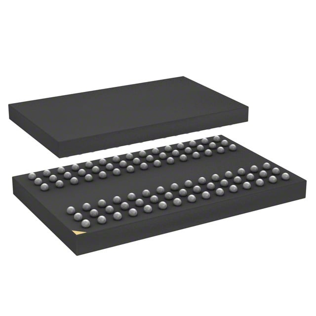
| Device Package | 90-TFBGA (8x13) | Memory Format | DRAM | Technology | SDRAM | ||
|---|---|---|---|---|---|---|---|
| Memory Size | 128 Mbit | Access Time | 5.4 ns | Grade | Automotive | ||
| Clock Frequency | 143 MHz | Voltage | 3V ~ 3.6V | Memory Type | Volatile | ||
| Operating Temperature | -40°C ~ 105°C (TA) | Write Cycle Time Word Page | N/A | Packaging | 90-TFBGA | ||
| Mounting Method | Volatile | Memory Interface | Parallel | Memory Organization | 4M x 32 | ||
| Moisture Sensitivity Level | 3 (168 Hours) | RoHS Compliance | ROHS3 Compliant | REACH Compliance | REACH Unaffected | ||
| Qualification | N/A | ECCN | EAR99 | HTS Code | 8542.32.0002 |
Overview of IS45S32400E-7BLA2 – IC DRAM 128MBIT PAR 90TFBGA
The IS45S32400E-7BLA2 is a 128Mbit synchronous DRAM organized as 4M × 32 with a quad-bank architecture and pipeline operation. It provides a parallel 32-bit interface and is designed for 3.3V memory systems requiring high-speed, fully synchronous DRAM operation.
Targeted at memory subsystems and embedded designs that need programmable burst controls, selectable CAS latencies, and standard LVTTL signalling, this device balances timing flexibility and density in a compact 90‑TFBGA (8×13) package.
Key Features
- Memory Core 4M × 32 organization delivering 128 Mbit density in a quad-bank SDRAM architecture for parallel 32-bit data transfers.
- Clock and Timing Supported clock frequencies include 166, 143 and 133 MHz; the -7 device is specified at 143 MHz with an access time from clock of 5.4 ns (CAS latency = 3).
- Programmable Burst & CAS Programmable burst lengths (1, 2, 4, 8, full page) and burst sequence (sequential/interleave); CAS latency selectable (2 or 3 clocks).
- Refresh and Power Auto Refresh and Self Refresh supported; 4096 refresh cycles with selectable refresh intervals (16 ms for A2 grade, 64 ms for Commercial/Industrial/A1 grades).
- Supply & I/O Single-power-supply operation at nominal 3.3V (3.0–3.6V range) with LVTTL-compatible interface signaling.
- Package & Temperature 90‑TFBGA (8×13) package; operating temperature range specified from −40 °C to 105 °C (TA) for the A2 option.
- System Capabilities Fully synchronous operation with all signals referenced to the rising clock edge and internal bank management for hiding row access/precharge.
Typical Applications
- 3.3V Memory Subsystems Works in systems designed for 3.3V SDRAM where a 128 Mbit parallel memory device is required.
- High‑speed Data Buffering Programmable burst modes and 32‑bit parallel interface support burst read/write and burst read/single write operations for buffering and burst transfers.
- Systems Requiring Robust Refresh Auto Refresh and Self Refresh with selectable refresh intervals (A2 vs Commercial/Industrial/A1) for designs with different retention and refresh timing needs.
Unique Advantages
- Flexible Timing Options: Selectable CAS latency (2 or 3) and multiple clock grade options enable tuning for latency vs. frequency trade-offs.
- Burst Transfer Efficiency: Programmable burst length and sequence provide control over sequential or interleaved access patterns to match system throughput requirements.
- Wide Parallel Data Path: 32‑bit data organization (4M × 32) simplifies integration into parallel memory buses and data‑width‑sensitive designs.
- Compact, High‑Density Package: 90‑TFBGA (8×13) reduces board area for high‑density memory layouts while maintaining thermal and signal integrity considerations for the package style.
- Extended Temperature Option: Availability up to −40 °C to 105 °C (TA) for the A2 option supports designs that require a wider operating temperature range.
Why Choose IS45S32400E-7BLA2?
The IS45S32400E-7BLA2 provides a compact, fully synchronous 128 Mbit SDRAM solution with configurable burst behavior, selectable CAS latency, and a 32‑bit parallel interface suitable for memory subsystems and embedded designs operating at 3.3V. Its quad‑bank, pipeline architecture and supported refresh modes deliver flexibility for designs balancing latency, throughput and retention needs.
This device is appropriate for engineering teams looking for a field‑proven SDRAM building block with clear timing grades and an extended temperature option, enabling scalable integration into designs that require standard LVTTL signalling and parallel data throughput in a 90‑TFBGA package.
Request a quote or submit an inquiry to receive pricing, availability and support information for the IS45S32400E-7BLA2.