IS45S32400E-7BLA2-TR
| Part Description |
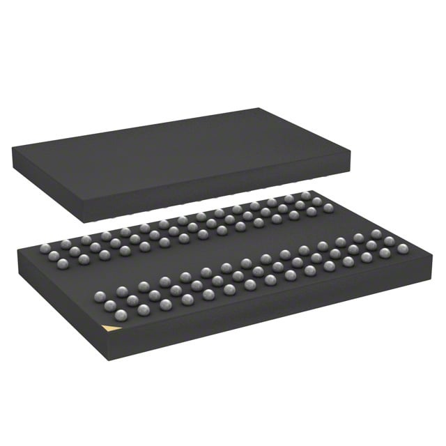
IC DRAM 128MBIT PAR 90TFBGA |
|---|---|
| Quantity | 511 Available (as of June 15, 2026) |

| Product Category | Memory |
|---|---|
| Manufacturer | Integrated Silicon Solution Inc |
| Manufacturing Status | Obsolete |
| Manufacturer Standard Lead Time | Contact Us |
| Datasheet |
Specifications & Environmental
| Device Package | 90-TFBGA (8x13) | Memory Format | DRAM | Technology | SDRAM | ||
|---|---|---|---|---|---|---|---|
| Memory Size | 128 Mbit | Access Time | 5.4 ns | Grade | Automotive | ||
| Clock Frequency | 143 MHz | Voltage | 3V ~ 3.6V | Memory Type | Volatile | ||
| Operating Temperature | -40°C ~ 105°C (TA) | Write Cycle Time Word Page | N/A | Packaging | 90-TFBGA | ||
| Mounting Method | Volatile | Memory Interface | Parallel | Memory Organization | 4M x 32 | ||
| Moisture Sensitivity Level | 3 (168 Hours) | RoHS Compliance | ROHS3 Compliant | REACH Compliance | REACH Unaffected | ||
| Qualification | N/A | ECCN | EAR99 | HTS Code | 8542.32.0002 |
Overview of IS45S32400E-7BLA2-TR – IC DRAM 128MBIT PAR 90TFBGA
The IS45S32400E-7BLA2-TR is a 128 Mbit synchronous DRAM (SDRAM) organized as 4M × 32 with a quad-bank architecture and pipeline operation. It provides high-speed, fully synchronous parallel memory suitable for systems that require a dedicated 128 Mbit SDRAM device with programmable burst and latency options.
Designed for systems operating with a 3.0 V – 3.6 V supply and a clock frequency up to 143 MHz (CL = 3), this device supports features such as internal bank management, programmable burst lengths, auto and self refresh modes, and a compact 90‑ball TF‑BGA package.
Key Features
- Core Architecture Quad-bank SDRAM configured as 1M × 32 × 4 banks to enable internal bank interleaving and row access/precharge hiding.
- Memory Organization & Capacity 128 Mbit total capacity organized as 4M × 32.
- SDRAM Timing & Performance Fully synchronous operation with clock-referenced inputs/outputs; supports 143 MHz operation with CAS latency = 3 and an access time from clock of 5.4 ns (CL = 3).
- Programmable Burst & Latency Programmable burst lengths (1, 2, 4, 8, full page) and burst sequencing (Sequential/Interleave); CAS latency programmable to 2 or 3 clocks.
- Refresh & Low Power Modes Supports Auto Refresh (CBR) and Self Refresh; refresh cycle options include 4096 refresh cycles per 16 ms (A2 grade) or 64 ms (Commercial/Industrial/A1 grade) as specified in device options.
- Interface LVTTL-compatible signals with parallel memory interface and support for random column address every clock cycle and burst termination commands (burst stop, precharge).
- Power Single power supply range of 3.0 V – 3.6 V (3.3 V ±0.3 V operation as specified in datasheet).
- Package & Temperature 90‑ball TF‑BGA (8 × 13) package with specified operating temperature range from -40°C to +105°C (TA).
Typical Applications
- System Memory Expansion Used as on‑board parallel SDRAM for systems that require an isolated 128 Mbit memory device with programmable burst and latency control.
- Embedded Memory Subsystems Suitable for embedded designs needing synchronous parallel DRAM with self-refresh and auto-refresh capabilities.
- High‑Speed Buffering Employed where pipeline architecture and quad‑bank operation support continuous high‑speed data transfers and random column access every clock cycle.
Unique Advantages
- Flexible Timing Control: Programmable CAS latency (2 or 3 clocks) and selectable burst lengths allow designers to tune throughput and latency to match system timing requirements.
- High‑Speed Synchronous Operation: Supports up to 143 MHz operation (CL = 3) with a 5.4 ns access time from clock, enabling responsive read/write bursts in synchronous systems.
- Robust Refresh Options: Auto and self refresh modes with device options for 4K refresh cycles per 16 ms or 64 ms provide flexibility for different refresh timing requirements.
- Compact, Board‑Level Package: 90‑TFBGA (8 × 13) ball array minimizes PCB footprint while supporting high‑density memory integration.
- Wide Supply Range: Operates across 3.0 V – 3.6 V, accommodating standard 3.3 V memory system rails.
- Wide Operating Temperature: Specified -40°C to +105°C (TA) for designs that require extended temperature operation.
Why Choose IS45S32400E-7BLA2-TR?
The IS45S32400E-7BLA2-TR positions itself as a straightforward, specification-driven SDRAM device offering 128 Mbit of organized memory in a quad‑bank, fully synchronous architecture. Its programmable latency and burst options, combined with internal bank management and refresh modes, make it suitable for designs that need predictable, clock‑synchronous memory behavior and flexible performance tuning.
This device is well suited to engineers designing systems around a parallel SDRAM memory interface who require a compact TF‑BGA package, a 3.0 V–3.6 V power envelope, and extended temperature operation. The clear, datasheet‑specified timing and refresh options support long‑term design planning and integration into established memory subsystems.
If you would like a quote or further purchasing information for the IS45S32400E-7BLA2-TR, please request a quote or contact sales for availability and lead‑time details.