IS45S32400E-7BLA1
| Part Description |
IC DRAM 128MBIT PAR 90TFBGA |
|---|---|
| Quantity | 566 Available (as of June 14, 2026) |

| Product Category | Memory |
|---|---|
| Manufacturer | Integrated Silicon Solution Inc |
| Manufacturing Status | Obsolete |
| Manufacturer Standard Lead Time | Contact Us |
| Datasheet |
Specifications & Environmental
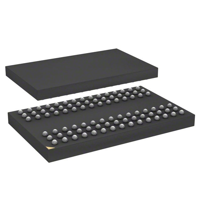
| Device Package | 90-TFBGA (8x13) | Memory Format | DRAM | Technology | SDRAM | ||
|---|---|---|---|---|---|---|---|
| Memory Size | 128 Mbit | Access Time | 5.4 ns | Grade | Industrial | ||
| Clock Frequency | 143 MHz | Voltage | 3V ~ 3.6V | Memory Type | Volatile | ||
| Operating Temperature | -40°C ~ 85°C (TA) | Write Cycle Time Word Page | N/A | Packaging | 90-TFBGA | ||
| Mounting Method | Volatile | Memory Interface | Parallel | Memory Organization | 4M x 32 | ||
| Moisture Sensitivity Level | 3 (168 Hours) | RoHS Compliance | ROHS Compliant | REACH Compliance | REACH Unaffected | ||
| Qualification | N/A | ECCN | EAR99 | HTS Code | 8542.32.0002 |
Overview of IS45S32400E-7BLA1 – 128Mbit SDRAM, 90‑TFBGA
The IS45S32400E-7BLA1 is a 128Mbit synchronous DRAM organized as 4M × 32 with a quad-bank architecture and pipeline operation. All I/O and control signals are fully synchronous to the rising clock edge to support deterministic high-speed data transfer.
Designed for systems that require a parallel SDRAM interface with programmable burst operation and low access latency, this device supports LVTTL signaling and operates from a single 3.3V power supply over an extended temperature range.
Key Features
- Core Architecture Quad-bank synchronous DRAM organized as 1M × 32 × 4 banks, enabling internal bank interleaving and hidden row access/precharge for continuous data flow.
- Memory Capacity & Organization 128 Mbit total capacity arranged as 4M × 32, providing a wide 32-bit data path for parallel memory subsystems.
- Performance Clock frequency options of 166, 143 and 133 MHz with programmable CAS latency of 2 or 3 clocks; typical access time from clock is 5.4 ns (CAS latency = 3, -7 speed grade).
- Burst & Sequencing Programmable burst lengths (1, 2, 4, 8, full page) and selectable sequential or interleave burst sequences; supports burst read/write and burst read/single write operations with burst termination commands.
- Refresh & Self-Refresh Auto Refresh and Self Refresh supported; refresh count options include 4K cycles per 64 ms for commercial/industrial/A1 grades or 4K per 16 ms for A2 grade as specified in the datasheet.
- Interface & Signaling LVTTL-compatible interface and parallel memory bus provide compatibility with 3.3V memory systems.
- Supply & Timing Single power supply: 3.3 V ±0.3 V (device supply range indicated as 3.0 V to 3.6 V in product specifications).
- Package & Temperature 90-ball TF‑BGA (8 × 13) package; operating temperature range shown as −40°C to +85°C (TA) for the specified part.
Typical Applications
- High‑speed memory subsystems Use where parallel SDRAM with programmable burst behavior and low CAS latency is required for sustained data throughput.
- Embedded processing platforms Suitable for embedded designs that need a 32-bit wide parallel memory interface and 128 Mbit capacity within a compact BGA package.
- Industrial systems Applicable in equipment that benefits from extended operating temperature support (−40°C to +85°C) and robust refresh management.
Unique Advantages
- Pipelined synchronous design: Enables deterministic timing with all signals referenced to the positive clock edge for predictable high-speed operation.
- Flexible burst control: Programmable burst lengths and sequences allow designers to tune memory transfers for throughput or latency as needed.
- Low-latency operation: CAS latency options (2 or 3 clocks) and access times down to 5.4 ns (from clock, CL=3, -7) reduce read latency in time-critical applications.
- Single-supply simplicity: Operation from a 3.3V supply simplifies power system design for standard memory rails.
- Compact BGA footprint: 90‑TFBGA (8×13) package balances board space with thermal and routing considerations for dense designs.
- Robust refresh options: Auto and self-refresh modes with documented refresh intervals support reliable data retention across grades.
Why Choose IC DRAM 128MBIT PAR 90TFBGA?
The IS45S32400E-7BLA1 delivers a combination of synchronous pipeline architecture, configurable burst operation, and low access latency in a compact 90‑TFBGA package. It is positioned for designs that require a 128 Mbit parallel SDRAM with predictable timing and flexible transfer modes.
This device is suitable for engineers seeking a 3.3V LVTTL-compatible SDRAM solution with extended temperature capability and documented timing/refresh behavior. It offers practical integration for systems needing a 32-bit wide parallel memory interface and programmable performance tuning.
Request a quote or submit an inquiry to check availability, lead times and pricing for IS45S32400E-7BLA1.