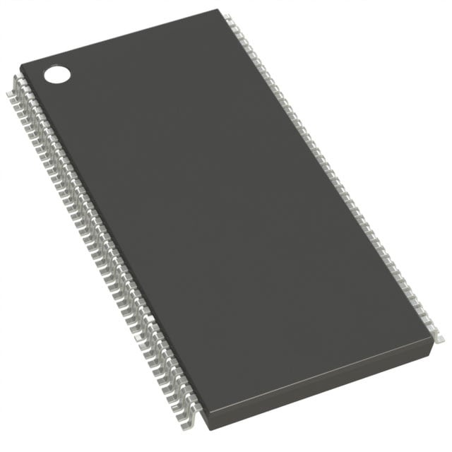
IS45S32400E-6TLA1-TR
| Part Description |
IC DRAM 128MBIT PAR 86TSOP II |
|---|---|
| Quantity | 27 Available (as of June 14, 2026) |

| Product Category | Memory |
|---|---|
| Manufacturer | Integrated Silicon Solution Inc |
| Manufacturing Status | Obsolete |
| Manufacturer Standard Lead Time | Contact Us |
| Datasheet |
Specifications & Environmental
| Device Package | 86-TSOP II | Memory Format | DRAM | Technology | SDRAM | ||
|---|---|---|---|---|---|---|---|
| Memory Size | 128 Mbit | Access Time | 5.4 ns | Grade | Industrial | ||
| Clock Frequency | 166 MHz | Voltage | 3V ~ 3.6V | Memory Type | Volatile | ||
| Operating Temperature | -40°C ~ 85°C (TA) | Write Cycle Time Word Page | N/A | Packaging | 86-TFSOP (0.400", 10.16mm Width) | ||
| Mounting Method | Volatile | Memory Interface | Parallel | Memory Organization | 4M x 32 | ||
| Moisture Sensitivity Level | 3 (168 Hours) | RoHS Compliance | ROHS3 Compliant | REACH Compliance | REACH Unaffected | ||
| Qualification | N/A | ECCN | EAR99 | HTS Code | 8542.32.0002 |
Overview of IS45S32400E-6TLA1-TR – IC DRAM 128MBIT PAR 86TSOP II
The IS45S32400E-6TLA1-TR is a 128Mbit synchronous DRAM (SDRAM) organized as 4M × 32 with four internal banks and a parallel memory interface. Built on a pipelined, fully synchronous architecture with LVTTL signaling, it is intended for high-speed memory subsystems that require predictable, clock-referenced data transfers.
This device targets designs operating from a 3.3V supply (3.3V ±0.3V / 3.0–3.6V) and supports industrial temperature operation to –40°C to +85°C in an 86‑pin TSOP-II package, balancing performance, integration density and package compactness.
Key Features
- Memory Architecture 128Mbit SDRAM organized as 4M × 32 with 4 internal banks for improved access concurrency and pipelined operation.
- Performance Clock-frequency options up to 166 MHz with an access time from clock of 5.4 ns (CAS latency = 3) for high-speed data throughput.
- Programmable Timing & Burst Programmable CAS latency (2 or 3 clocks), programmable burst lengths (1, 2, 4, 8, full page) and selectable burst sequence (sequential/interleave) for flexible timing and transfer modes.
- Refresh & Self-Refresh Auto-Refresh and Self-Refresh support with 4,096 refresh cycles; refresh period selectable as 16 ms (A2 grade) or 64 ms (Commercial/Industrial/A1 grades) as specified.
- Interface & Signaling Parallel memory interface with LVTTL-compatible I/O referenced to the positive clock edge for synchronous operation.
- Power Single power supply operation: 3.3V ±0.3V (listed supply range 3.0–3.6V) for standard 3.3V memory systems.
- Package & Temperature Available in an 86‑TSOP II (86‑TFSOP, 0.400", 10.16 mm width) package and rated for operation from –40°C to +85°C (TA) where specified.
Typical Applications
- Memory subsystems Acts as synchronous DRAM storage in systems requiring 128Mbit parallel SDRAM with predictable clocked timing.
- High-speed buffering Used where pipelined, banked SDRAM access and programmable burst transfers improve throughput for data buffering.
- Embedded 3.3V designs Suited to embedded systems designed around a 3.3V memory VDD using LVTTL signaling and a parallel SDRAM interface.
Unique Advantages
- High-frequency operation: Supports up to 166 MHz clocking with low access time (5.4 ns at CAS‑3), enabling faster synchronous transfers.
- Flexible transfer modes: Programmable CAS latency, burst length and burst sequence allow tuning for a variety of access patterns and system timing requirements.
- Quad-bank architecture: Four internal banks provide improved concurrency and reduced row-precharge penalties for sustained data throughput.
- Standard 3.3V supply: Operates from 3.3V (3.0–3.6V range), simplifying integration into established 3.3V memory subsystems.
- Industrial temperature rating: Specified for –40°C to +85°C (TA) to support applications that require extended temperature operation.
- Compact TSOP-II package: 86‑pin TSOP-II (0.400", 10.16 mm width) reduces PCB area while providing a full 32‑bit data path.
Why Choose IC DRAM 128MBIT PAR 86TSOP II?
The IS45S32400E-6TLA1-TR delivers a synchronous, pipelined 128Mbit DRAM solution with programmable timing and burst capabilities for designers who need predictable, clocked memory behavior. Its 4M × 32 organization, quad-bank architecture and LVTTL interface make it suitable for 3.3V memory subsystems requiring parallel SDRAM at up to 166 MHz.
With industrial temperature coverage and an 86‑TSOP II package, this device is appropriate for compact boards and systems demanding robust, high-speed DRAM integration backed by ISSI’s product documentation and specification support.
Request a quote or contact sales to discuss availability, lead times and pricing for the IS45S32400E-6TLA1-TR.