IS45S32400E-7TLA1
| Part Description |
IC DRAM 128MBIT PAR 86TSOP II |
|---|---|
| Quantity | 1,010 Available (as of June 12, 2026) |
| Product Category | Memory |
|---|---|
| Manufacturer | Integrated Silicon Solution Inc |
| Manufacturing Status | Obsolete |
| Manufacturer Standard Lead Time | Contact Us |
| Datasheet |
Specifications & Environmental
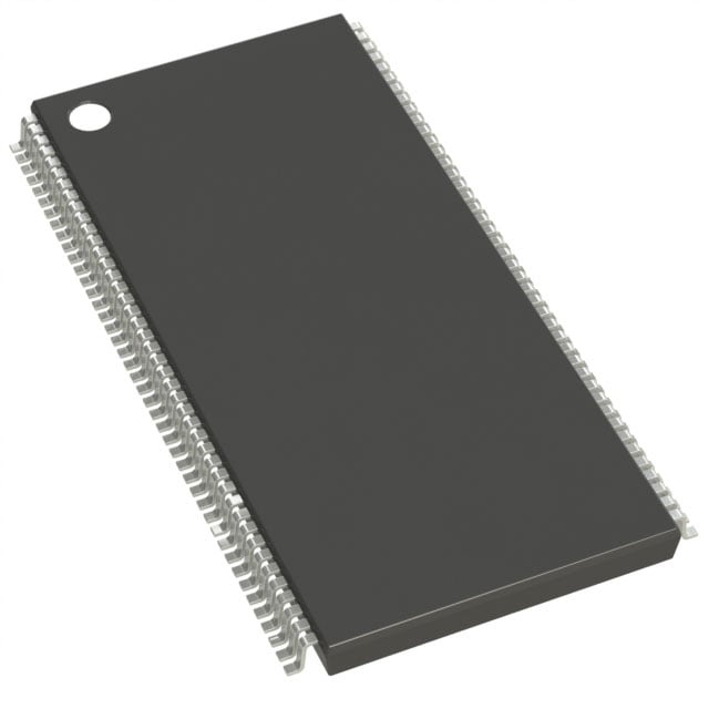
| Device Package | 86-TSOP II | Memory Format | DRAM | Technology | SDRAM | ||
|---|---|---|---|---|---|---|---|
| Memory Size | 128 Mbit | Access Time | 5.4 ns | Grade | Industrial | ||
| Clock Frequency | 143 MHz | Voltage | 3V ~ 3.6V | Memory Type | Volatile | ||
| Operating Temperature | -40°C ~ 85°C (TA) | Write Cycle Time Word Page | N/A | Packaging | 86-TFSOP (0.400", 10.16mm Width) | ||
| Mounting Method | Volatile | Memory Interface | Parallel | Memory Organization | 4M x 32 | ||
| Moisture Sensitivity Level | 3 (168 Hours) | RoHS Compliance | ROHS3 Compliant | REACH Compliance | REACH Unaffected | ||
| Qualification | N/A | ECCN | EAR99 | HTS Code | 8542.32.0002 |
Overview of IS45S32400E-7TLA1 – IC DRAM 128MBIT PAR 86TSOP II
The IS45S32400E-7TLA1 is a 128Mbit synchronous DRAM organized as 4M × 32 with a quad-bank architecture and pipeline internal operation. It is a parallel SDRAM device designed for 3.3V memory systems and optimized for high-speed, fully synchronous data transfers.
This device targets designs that require low-latency, high-throughput parallel DRAM with programmable burst and timing options, delivered in an 86-pin TSOP-II package and specified for -40°C to +85°C operation.
Key Features
- Core Architecture Quad-bank synchronous DRAM organized as 4M × 32 (1M × 32 × 4 banks) enabling internal bank operation for hiding row access and precharge.
- Memory Capacity & Format 128 Mbit total memory capacity in DRAM format providing parallel data paths for fast transfers.
- Performance Grades Available clock-frequency grades including 166, 143 and 133 MHz; the -7 grade provides a 143 MHz clock with access time from clock of 5.4 ns at CAS latency = 3.
- Programmable Burst & Timing Programmable burst lengths (1, 2, 4, 8, full page), burst sequence (sequential/interleave), and CAS latency options (2 or 3 clocks) for flexible timing and throughput tuning.
- Refresh & Self-Refresh Auto Refresh (CBR) and Self Refresh supported; 4,096 refresh cycles with refresh intervals of 16 ms (A2 grade) or 64 ms (Commercial/Industrial/A1 grade).
- Interface & Signaling Fully synchronous operation with all signals referenced to the positive clock edge and LVTTL-compatible interface for parallel memory systems.
- Power Single power supply operation at 3.3 V ±0.3 V (specified 3.0 V to 3.6 V).
- Package & Temperature Supplied in an 86-pin TSOP-II (86-TFSOP, 0.400", 10.16 mm width) package and specified for -40°C to +85°C ambient temperature (TA).
- Burst Operations & Termination Supports burst read/write and burst read/single write operations with burst termination via burst stop and precharge commands.
Typical Applications
- High-speed memory subsystems As parallel SDRAM in systems that require synchronous, low-latency data transfers and banked memory access.
- Buffer and frame memory For designs that need programmable burst lengths and sequence control to manage contiguous or interleaved data streams.
- 3.3V memory designs Integrates into 3.3 V VDD memory systems where a single 3.3 V supply and LVTTL interface are required.
- Industrial-temperature embedded systems Suitable for applications requiring operation across -40°C to +85°C ambient temperature.
Unique Advantages
- Synchronous pipeline architecture: Internal pipeline and bank organization enable high-speed data transfer referenced to the positive clock edge.
- Flexible timing control: Programmable CAS latency (2 or 3 clocks) and multiple burst modes let designers optimize latency versus throughput.
- Multiple frequency options: Offered in 166, 143 and 133 MHz grades to match system timing requirements; the -7 grade provides 143 MHz performance with 5.4 ns access time at CL=3.
- Robust refresh modes: Auto Refresh and Self Refresh with selectable refresh intervals (16 ms or 64 ms) accommodate varied system refresh policies.
- Industry-standard package: 86-pin TSOP-II footprint (0.400", 10.16 mm width) simplifies board-level integration for parallel memory designs.
Why Choose IS45S32400E-7TLA1?
The IS45S32400E-7TLA1 combines a 128 Mbit density and quad-bank SDRAM architecture with programmable burst and timing options to provide configurable, high-speed parallel memory. Its fully synchronous interface, LVTTL signaling, and multiple frequency grades make it suitable for systems that need deterministic timing and flexible throughput options.
Specified for operation from -40°C to +85°C and powered from a single 3.3 V supply (3.0 V to 3.6 V), this device is intended for designers seeking a reliable, configurable 128Mb SDRAM in an 86-pin TSOP-II package backed by ISSI device specifications.
Request a quote or submit a sales inquiry for IS45S32400E-7TLA1 to obtain pricing and availability information.