IS45S32400E-7TLA2
| Part Description |
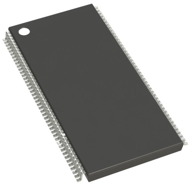
IC DRAM 128MBIT PAR 86TSOP II |
|---|---|
| Quantity | 1,830 Available (as of June 10, 2026) |

| Product Category | Memory |
|---|---|
| Manufacturer | Integrated Silicon Solution Inc |
| Manufacturing Status | Obsolete |
| Manufacturer Standard Lead Time | Contact Us |
| Datasheet |
Specifications & Environmental
| Device Package | 86-TSOP II | Memory Format | DRAM | Technology | SDRAM | ||
|---|---|---|---|---|---|---|---|
| Memory Size | 128 Mbit | Access Time | 5.4 ns | Grade | Automotive | ||
| Clock Frequency | 143 MHz | Voltage | 3V ~ 3.6V | Memory Type | Volatile | ||
| Operating Temperature | -40°C ~ 105°C (TA) | Write Cycle Time Word Page | N/A | Packaging | 86-TFSOP (0.400", 10.16mm Width) | ||
| Mounting Method | Volatile | Memory Interface | Parallel | Memory Organization | 4M x 32 | ||
| Moisture Sensitivity Level | 3 (168 Hours) | RoHS Compliance | ROHS Compliant | REACH Compliance | REACH Unaffected | ||
| Qualification | N/A | ECCN | EAR99 | HTS Code | 8542.32.0002 |
Overview of IS45S32400E-7TLA2 – IC DRAM 128MBIT PAR 86TSOP II
The IS45S32400E-7TLA2 is a 128Mbit synchronous DRAM organized as 4M × 32 with a quad-bank, pipelined architecture. It is a parallel-interface SDRAM designed for use in 3.3V memory systems where fully synchronous, clock-referenced operation and programmable burst access are required.
Typical deployment is in systems that require high-speed, pipelined SDRAM access with flexible burst and latency configuration, supported by a standard 86‑pin TSOP II package and extended operating temperature up to -40°C to +105°C (TA).
Key Features
- Core Architecture Quad-bank SDRAM internally organized as 1M × 32 × 4 banks to support hidden row access/precharge and pipelined high-speed transfers.
- Synchronous Operation Fully synchronous device with all signals referenced to the positive clock edge; LVTTL interface.
- Performance Clock frequency option at 143 MHz (‑7 speed grade) with programmable CAS latency (2 or 3 clocks) and an access time of 5.4 ns at CAS latency = 3.
- Burst and Column Flexibility Programmable burst length (1, 2, 4, 8, full page), sequential/interleave burst sequence, and random column address every clock cycle for flexible data-transfer patterns.
- Refresh and Self-Refresh Supports Auto Refresh (CBR) and Self Refresh; 4096 refresh cycles per refresh period (A2 grade: 16 ms; Commercial/Industrial/A1 grade: 64 ms) as specified in the datasheet.
- Power Single power supply operation at 3.3 V (3.0–3.6 V supply range).
- Package and Mounting Supplied in an 86‑TSOP II (86‑TFSOP, 0.400" / 10.16 mm width) package suitable for standard surface-mount assembly.
- Temperature Range Operating ambient range documented at -40°C to +105°C (TA) for the specified device variant.
Typical Applications
- 3.3 V memory subsystems Acts as synchronous DRAM in 3.3 V memory systems requiring 128 Mbit density and quad-bank operation.
- High-speed burst data buffering Programmable burst lengths and CAS latency options enable adaptable buffering for designs needing burst read/write capability.
- Temperature-challenged environments Devices with the documented -40°C to +105°C operating range are suitable where extended ambient temperature support is required.
Unique Advantages
- Fully synchronous, clock-referenced design: Ensures deterministic timing with all signals referenced to the positive clock edge for predictable system integration.
- Flexible performance configuration: Multiple clock-frequency grades and programmable CAS latency (2 or 3) let designers trade latency and throughput per application needs.
- Burst and access flexibility: Programmable burst length and sequence plus random column addressing every clock cycle simplify varied data-transfer patterns.
- Integrated refresh management: Auto Refresh and Self Refresh support with documented refresh cycles (4K) and timing options by grade.
- Industry-standard package: 86‑TSOP II footprint (10.16 mm width) for straightforward board-level integration and assembly.
- 3.3 V single-supply operation: Matches common 3.3 V memory system rails (3.0–3.6 V supply range) for compatibility with standard power domains.
Why Choose IS45S32400E-7TLA2?
The IS45S32400E-7TLA2 positions itself as a specification-driven 128Mbit SDRAM option for designs that require fully synchronous, programmable burst operation and quad-bank architecture. Its documented timing (5.4 ns access at CL=3), 143 MHz speed grade, and LVTTL interface provide predictable performance for systems built around 3.3 V memory rails.
With Auto Refresh/Self Refresh support, flexible burst and CAS settings, and an 86‑TSOP II package, this device is suited to engineers seeking a well-documented SDRAM component for memory subsystems that demand configurability and extended ambient temperature capability.
Request a quote or submit an inquiry to get pricing, availability, and detailed ordering information for the IS45S32400E-7TLA2.