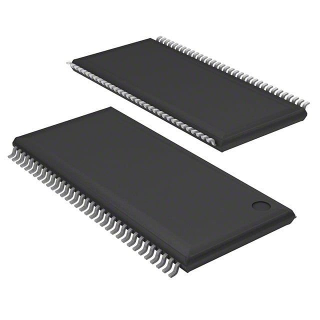
IS46R16320D-6TLA2
| Part Description |
IC DRAM 512MBIT PAR 66TSOP II |
|---|---|
| Quantity | 188 Available (as of June 12, 2026) |

| Product Category | Memory |
|---|---|
| Manufacturer | Integrated Silicon Solution Inc |
| Manufacturing Status | Obsolete |
| Manufacturer Standard Lead Time | Contact Us |
| Datasheet |
Specifications & Environmental
| Device Package | 66-TSOP II | Memory Format | DRAM | Technology | SDRAM - DDR | ||
|---|---|---|---|---|---|---|---|
| Memory Size | 512 Mbit | Access Time | 700 ps | Grade | Automotive | ||
| Clock Frequency | 166 MHz | Voltage | 2.3V ~ 2.7V | Memory Type | Volatile | ||
| Operating Temperature | -40°C ~ 105°C (TA) | Write Cycle Time Word Page | 15 ns | Packaging | 66-TSSOP (0.400", 10.16mm Width) | ||
| Mounting Method | Volatile | Memory Interface | Parallel | Memory Organization | 32M x 16 | ||
| Moisture Sensitivity Level | 3 (168 Hours) | RoHS Compliance | ROHS Compliant | REACH Compliance | REACH Unaffected | ||
| Qualification | N/A | ECCN | EAR99 | HTS Code | 8542.32.0028 |
Overview of IS46R16320D-6TLA2 – 512Mbit DDR SDRAM (32M × 16), 66‑TSOP II
The IS46R16320D-6TLA2 is a 512‑Mbit double‑data‑rate (DDR) SDRAM device organized as 32M × 16 with a parallel memory interface. It implements a pipelined DDR architecture with two data transfers per clock cycle and internal DLL to align data and strobe timing for high‑speed operation.
Designed for systems that require high throughput and flexible timing, the device offers programmable burst lengths and CAS latencies, SSTL_2 compatible I/O, and a compact 66‑TSOP II package with an extended operating range down to −40°C and up to 105°C.
Key Features
- Core Architecture Double‑data‑rate pipeline architecture with two data transfers per clock cycle; DLL aligns DQ/DQS transitions with CLK and commands are registered on positive CLK edges.
- Memory Organization 512 Mbit capacity arranged as 32M × 16 with four internal banks (four banks of 128Mb) to allow concurrent operations and continuous read/write burst accesses.
- Performance & Timing Rated for a clock frequency up to 166 MHz with an access time of 700 ps and a word page write cycle time of 15 ns. Supports burst lengths of 2, 4 and 8 and programmable CAS latencies of 2, 2.5 and 3.
- I/O and Interface SSTL_2 compatible I/O, differential clock inputs (CK and /CK), bidirectional data strobe (DQS) edge/centre alignment for READ/WRITE, and Data Mask (DM) that masks write data on both DQS edges.
- Refresh and Power Management Auto Refresh and Self Refresh modes, Auto Precharge, and tRAS lockout support help maintain data integrity across operating conditions.
- Power Supply Operates from a 2.3 V to 2.7 V supply range (VDD and VDDQ ranges per device option), compatible with SSTL_2 signaling levels.
- Package & Temperature 66‑TSSOP (66‑TSOP II) package (0.400" / 10.16 mm width) and an operating temperature range of −40°C to +105°C (TA).
Typical Applications
- High‑speed buffering and data capture DDR bursts and programmable timing support continuous read/write operations where sustained throughput is required.
- Embedded memory subsystems Compact 66‑TSOP II footprint and 512 Mbit density for designs needing parallel DDR SDRAM in space‑constrained boards.
- Systems requiring SSTL_2 I/O SSTL_2 compatible signaling and differential clock inputs enable integration with interfaces that rely on SSTL_2 levels and differential timing.
Unique Advantages
- Two transfers per clock cycle Double‑data‑rate operation effectively doubles data throughput without increasing clock rate.
- Flexible burst and latency options Programmable burst lengths (2/4/8) and CAS latencies (2, 2.5, 3) let designers tune performance for specific access patterns.
- SSTL_2 compatible I/O with DQS support Edge‑ and centre‑aligned DQS handling simplifies timing alignment for both reads and writes and supports robust capture of DDR data.
- Compact package with wide temperature window 66‑TSOP II package and −40°C to +105°C operating range enable deployment in temperature‑sensitive and space‑limited designs.
- Built‑in refresh and power modes Auto Refresh, Self Refresh and Auto Precharge modes reduce system intervention for data retention and power management.
Why Choose IC DRAM 512MBIT PAR 66TSOP II?
The IS46R16320D-6TLA2 positions itself as a practical 512‑Mbit DDR SDRAM option where compact package size, flexible timing and SSTL_2‑compatible I/O are required. Its DDR pipeline architecture, programmable latency and burst features provide designers with the control needed to optimize throughput and access patterns.
This device is suitable for designs that need parallel DDR memory in a 66‑TSOP II footprint and a broad operating temperature range. The combination of refresh modes, differential clocking and DQS timing support delivers a straightforward memory building block for systems prioritizing deterministic timing and sustained data transfers.
Request a quote or submit an inquiry for IS46R16320D-6TLA2 to receive pricing, availability and lead‑time information.