IS46R86400D-6TLA1
| Part Description |
IC DRAM 512MBIT PAR 66TSOP II |
|---|---|
| Quantity | 141 Available (as of June 10, 2026) |

| Product Category | Memory |
|---|---|
| Manufacturer | Integrated Silicon Solution Inc |
| Manufacturing Status | Obsolete |
| Manufacturer Standard Lead Time | Contact Us |
| Datasheet |
Specifications & Environmental
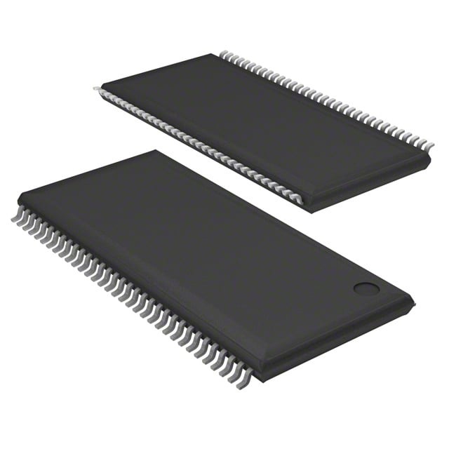
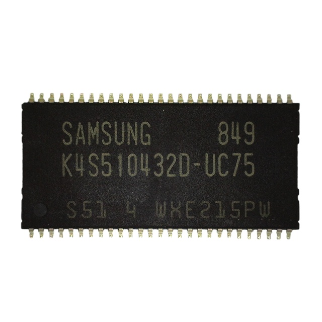
| Device Package | 66-TSOP II | Memory Format | DRAM | Technology | SDRAM - DDR | ||
|---|---|---|---|---|---|---|---|
| Memory Size | 512 Mbit | Access Time | 700 ps | Grade | Industrial | ||
| Clock Frequency | 166 MHz | Voltage | 2.3V ~ 2.7V | Memory Type | Volatile | ||
| Operating Temperature | -40°C ~ 85°C (TA) | Write Cycle Time Word Page | 15 ns | Packaging | 66-TSSOP (0.400", 10.16mm Width) | ||
| Mounting Method | Volatile | Memory Interface | Parallel | Memory Organization | 64M x 8 | ||
| Moisture Sensitivity Level | 3 (168 Hours) | RoHS Compliance | ROHS Compliant | REACH Compliance | REACH Unaffected | ||
| Qualification | N/A | ECCN | EAR99 | HTS Code | 8542.32.0028 |
Overview of IS46R86400D-6TLA1 – 512 Mbit DDR SDRAM, 66‑TSOP II
The IS46R86400D-6TLA1 is a 512‑Mbit DDR SDRAM organized as 64M × 8 with a parallel memory interface. It implements a double‑data‑rate pipeline architecture with four internal banks and SSTL_2 compatible I/O for high‑speed, burst‑oriented memory operations.
This device is available in a 66‑pin TSOP‑II package and supports a supply range of 2.3 V to 2.7 V, an operating temperature range of -40°C to +85°C, and a maximum clock frequency of 166 MHz for the -6 speed grade.
Key Features
- Core Architecture Double‑data‑rate (DDR) pipeline architecture enabling two data transfers per clock cycle and four internal banks for concurrent operation.
- Memory Organization & Density 512 Mbit capacity organized as 64M × 8, internally arranged as four banks of 128 Mb each.
- Performance & Timing Maximum clock frequency up to 166 MHz (‑6 speed grade); access time 700 ps and write cycle time (word/page) of 15 ns. Programmable CAS latency options include 2, 2.5 and 3.
- Data Transfer & Burst Control Burst Length options 2, 4 and 8 with sequential and interleave burst types; read/write bursts use DQS (data strobe) for captured data alignment.
- Interface & Signaling SSTL_2 compatible I/O, differential clock inputs (CK/CK̄), DLL to align DQ/DQS with clock, and Data Mask (DM) that masks write data on both DQS edges.
- Refresh & Power Modes Supports Auto Refresh and Self Refresh modes and Auto Precharge to manage refresh requirements and power states.
- Package & Mounting 66‑TSSOP / 66‑TSOP II package with 0.400" (10.16 mm) body width, surface‑mount mounting type.
- Supply & Temperature VDD and VDDQ supply range 2.3 V to 2.7 V (VDD/VDDQ 2.5 V ±0.2 V for -6 option) and operating temperature -40°C to +85°C (TA) for industrial range.
Typical Applications
- Embedded memory subsystems — Provides 512‑Mbit DDR storage in a 66‑TSOP II form factor for embedded boards and modules requiring parallel DDR SDRAM.
- Industrial and commercial equipment — Industrial temperature support (‑40°C to +85°C) and SSTL_2 I/O make the device suitable for systems operating across extended temperature ranges.
- High‑speed buffering and burst storage — DDR architecture, programmable CAS latency and burst length options enable high‑throughput burst read/write operations for buffer memory functions.
Unique Advantages
- Double‑data‑rate throughput: Two data transfers per clock cycle increase effective bandwidth without raising clock frequency.
- Flexible timing and burst control: Programmable CAS latencies and selectable burst lengths (2/4/8) let designers tune latency and throughput to system requirements.
- SSTL_2 compatible I/O with differential clocking: Differential CK/CK̄ and DLL alignment improve timing margin for high‑speed interfaces.
- Compact TSOP‑II package: 66‑pin TSOP‑II (0.400", 10.16 mm width) provides a low‑profile, surface‑mount option for space‑constrained PCBs.
- Extended operating range: 2.3 V–2.7 V supply tolerance and ‑40°C to +85°C operating temperature support robust operation across commercial and industrial environments.
Why Choose IS46R86400D-6TLA1?
The IS46R86400D-6TLA1 delivers a compact 512‑Mbit DDR SDRAM solution with DDR pipeline architecture and SSTL_2‑compatible I/O for reliable, high‑speed burst transfers. Its programmable latency, burst control and built‑in timing features (DLL, DQS alignment) make it suitable for designs that require predictable timing and efficient throughput in a small TSOP‑II package.
Engineers building embedded systems, industrial controllers or memory buffer subsystems will find this device offers a balance of performance, supply tolerance (2.3 V–2.7 V) and an extended operating temperature range for durable, long‑lifecycle designs.
Request a quote or contact sales to check availability, pricing and lead times for the IS46R86400D-6TLA1.