
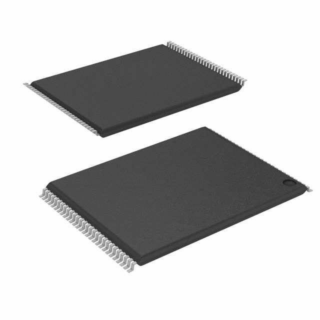
M30LW128D110N6
| Part Description |
IC FLASH 128MBIT PARALLEL 56TSOP |
|---|---|
| Quantity | 1,981 Available (as of June 15, 2026) |
| Product Category | Memory |
|---|---|
| Manufacturer | STMicroelectronics |
| Manufacturing Status | Obsolete |
| Manufacturer Standard Lead Time | Contact Us |
| Datasheet |
Specifications & Environmental
| Device Package | 56-TSOP | Memory Format | FLASH | Technology | FLASH | ||
|---|---|---|---|---|---|---|---|
| Memory Size | 128 Mbit | Access Time | 110 ns | Grade | Industrial | ||
| Clock Frequency | N/A | Voltage | 2.7V ~ 3.6V | Memory Type | Non-Volatile | ||
| Operating Temperature | -40°C ~ 85°C (TA) | Write Cycle Time Word Page | 110 ns | Packaging | 56-TFSOP (0.724", 18.40mm Width) | ||
| Mounting Method | Non-Volatile | Memory Interface | Parallel | Memory Organization | 8M x 8 x 2, 4M x 16 | ||
| Moisture Sensitivity Level | 1 (Unlimited) | RoHS Compliance | ROHS Compliant | REACH Compliance | REACH Unaffected | ||
| Qualification | N/A | ECCN | OBSOLETE | HTS Code | 8542.32.0071 |
Overview of M30LW128D110N6 – 128 Mbit Parallel Flash, 56‑TSOP
The M30LW128D110N6 is a 128 Mbit non-volatile flash memory in a 56‑TSOP package, implemented as two stacked 64 Mbit devices. It provides a parallel x8 or x16 data bus and a command-driven flash architecture suited for systems that require parallel high‑bandwidth code or data storage.
Key value comes from flexible bus width (x8/x16), a 2.7 V–3.6 V main supply with VDDQ support for I/O buffer voltages, and block‑oriented erase/program capabilities that support suspend/resume and protection features for robust in‑system memory management.
Key Features
- Memory Density and Organization — 128 Mbit total capacity implemented as two stacked 64 Mbit devices; memory organization options include 8M × 8 × 2 or 4M × 16.
- Parallel Interface and Bus Width — Wide x8 or x16 data bus for high bandwidth parallel read/write operations and flexible system integration.
- Supply and I/O Voltages — VDD supply range 2.7 V to 3.6 V for program, erase and read; VDDQ for I/O buffers configurable from 1.8 V up to VDD.
- Performance — Random read access time 110 ns; page mode read supports 110/25 ns timing; write cycle time (word/page) 110 ns.
- Program/Erase and Endurance — 16‑word write buffer with 16 µs effective word programming time and a typical program/erase endurance of 100,000 cycles per block.
- Block Architecture and Protection — 128 uniform 64 KWord / 128 KByte blocks with block protect/unprotect commands and a 128‑bit protection register for access control.
- Program/Erase Control — Support for program and erase suspend/resume operations and status register reporting (Ready/Busy, program/erase status bits).
- Package and Temperature — Supplied in a 56‑TFSOP/TSOP56 (0.724", 18.40 mm width) package; operating temperature range −40 °C to 85 °C.
Typical Applications
- Embedded systems requiring parallel code storage — Provides non‑volatile parallel storage for systems that need wide‑bus reads for fast code fetch or data access.
- Boot and firmware storage — Two‑die stacking and block architecture enable large uniform blocks suitable for storing firmware images with block protection options.
- High‑bandwidth data logging — x8/x16 bus and page mode read timings support designs that require sustained parallel read/write throughput.
Unique Advantages
- Stacked dual‑die configuration — Two M58LW064D 64 Mbit devices in one package deliver 128 Mbit capacity while maintaining uniform block layout for simplified memory management.
- Flexible bus operation (x8/x16) — Selectable data bus width allows designers to match system bus requirements and maximize throughput where a wide parallel interface is available.
- Wide supply and I/O voltage support — VDD 2.7 V–3.6 V and VDDQ programmable from 1.8 V to VDD support adapter designs with different I/O voltage domains.
- Block‑level robustness — 128 uniform blocks and a 128‑bit protection register enable granular protection and management for in‑field updates and secure storage.
- Program/erase suspend and status reporting — Suspend/resume capability and a detailed status register allow deterministic handling of long program/erase operations in system control flows.
- Industrial temperature range — Specified operation from −40 °C to 85 °C for use in temperature‑sensitive embedded applications.
Why Choose M30LW128D110N6?
The M30LW128D110N6 positions itself as a high‑capacity parallel flash memory optimized for applications that need wide‑bus access, block‑level control, and flexible I/O voltage support. Its stacked 64 Mbit die approach and uniform block architecture make memory partitioning, protection and in‑system updates straightforward for embedded designers.
This device is suitable for teams designing systems that rely on parallel flash for code or large data storage, where predictable read timings, block protection and program/erase control are required. The combination of supply flexibility, endurance figures, and suspend/resume capabilities supports longer product life and maintainability in deployed systems.
Request a quote or submit an inquiry to receive pricing, availability and lead‑time information for the M30LW128D110N6.


Date Founded: 1987
Headquarters: Plan-les-Ouates, Geneva, Switzerland
Employees: 50,000+
Revenue: $17.24 Billion
Certifications and Memberships: ISO9001:2015, ISO14001:2015, ISO45001:2018, IATF16949:2016, ISO50001:2018


