
M52D2561616A-6BG2F
| Part Description |
LPSDR SDRAM 256Mbit, 166MHz, 1.8V, 54-Ball FBGA |
|---|---|
| Quantity | 537 Available (as of June 15, 2026) |

| Product Category | Memory |
|---|---|
| Manufacturer | ESMT |
| Manufacturing Status | MP |
| Manufacturer Standard Lead Time | Contact Us |
| Datasheet |
Specifications & Environmental
| Device Package | 54-FBGA (8x8) | Memory Format | DRAM | Technology | DRAM | ||
|---|---|---|---|---|---|---|---|
| Memory Size | 256 Mbit | Access Time | 5.4 ns | Grade | Commercial | ||
| Clock Frequency | 166 MHz | Voltage | 1.7V ~ 1.95V | Memory Type | Volatile | ||
| Operating Temperature | 0°C – 70°C | Write Cycle Time Word Page | 12 ns | Packaging | 54-FBGA | ||
| Mounting Method | Surface Mount | Memory Interface | LVCMOS | Memory Organization | 4M x 16 | ||
| Moisture Sensitivity Level | 3 | RoHS Compliance | Compliant | REACH Compliance | REACH Unknown | ||
| Qualification | JEDEC | ECCN | EAR99 | HTS Code | 8542.32.00.24 |
Overview of M52D2561616A-6BG2F – LPSDR SDRAM 256Mbit, 166MHz, 1.8V, 54-Ball FBGA
The M52D2561616A-6BG2F is a 268,435,456‑bit mobile synchronous DRAM organized as 4 × 4,194,304 words by 16 bits with four internal banks. It delivers synchronous high‑data‑rate operation at a rated clock frequency of 166 MHz and is optimized for high‑bandwidth, high‑performance memory system applications.
Designed for low‑voltage systems, this commercial‑grade device supports multiplexed addressing, programmable burst lengths and latencies, and standard JEDEC compliance for straightforward integration into compact, surface‑mount designs.
Key Features
- Memory Organization 268,435,456 bits organized as 4M × 16 with four banks, providing predictable, banked access for high throughput.
- Clock and Timing Rated for 166 MHz operation with access time of 5.4 ns and a write cycle time (word/page) of 12 ns; all inputs are sampled on the positive edge of the system clock.
- Low‑Voltage Operation 1.8V nominal supply with an operating range of 1.7V to 1.95V to support low‑power system designs.
- Programmable Performance CAS Latency (3) and selectable burst lengths (1, 2, 4, 8, and full page) plus burst type (sequential and interleave) for flexible performance tuning.
- Interface and Control LVCMOS compatible interface with standard command signals (CLK, CS, CKE, RAS, CAS, WE) and DQ0–DQ15 data lines; DQM supports data masking.
- Refresh and Self‑Refresh Auto and self refresh support with a 64 ms refresh period (8K cycles); features include PASR and TCSR for power‑aware refresh management.
- Driver and Signal Control Supports Driver Strength (DS) programming and EMRS/MRS cycles for device configuration.
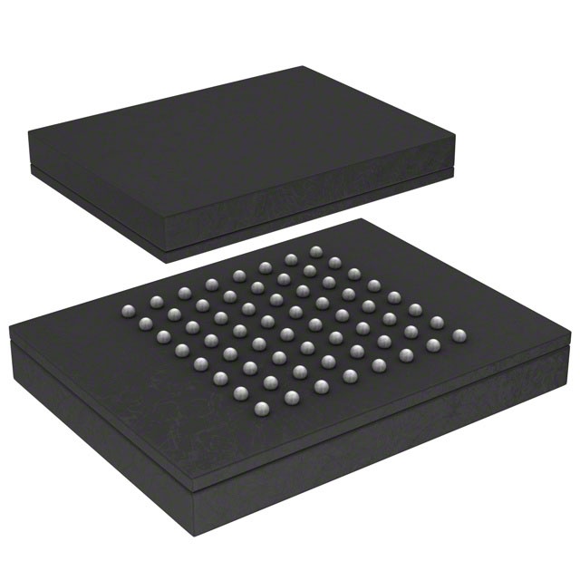
- Package and Mounting 54‑ball FBGA (8 mm × 8 mm × 1 mm body, 0.8 mm ball pitch), surface‑mount package suitable for compact PCB layouts.
- Commercial Grade & Compliance JEDEC qualification and RoHS compliance for commercial applications; operating temperature range 0 °C to 70 °C.
Typical Applications
- High‑bandwidth memory systems — Delivers synchronous, banked DRAM performance for systems that require predictable high throughput.
- Low‑voltage embedded designs — 1.8V operation supports power‑sensitive platforms where reduced supply voltage is required.
- Compact surface‑mount boards — 54‑ball FBGA package enables integration into space‑constrained PCBs.
Unique Advantages
- Four‑bank architecture: Enables concurrent bank operations to improve effective throughput in multi‑access scenarios.
- Flexible burst and latency settings: Programmable burst lengths and CAS Latency (3) let designers match memory timing to system requirements.
- Low‑voltage operation: 1.7V–1.95V supply range reduces system power consumption compared with higher‑voltage alternatives.
- Positive‑edge synchronous sampling: All inputs are sampled on the rising clock edge for predictable timing relationships in synchronous systems.
- Compact FBGA footprint: 54‑ball, 8 mm × 8 mm body with 0.8 mm ball pitch minimizes PCB area while maintaining robust connectivity.
- Standards and environmental compliance: JEDEC qualification and RoHS compliance support lifecycle and regulatory considerations for commercial products.
Why Choose M52D2561616A-6BG2F?
The M52D2561616A-6BG2F from ESMT is positioned for designers who need a synchronous, low‑voltage DRAM solution with flexible timing and burst options in a compact package. Its four‑bank organization and 166 MHz rating provide a balance of bandwidth and configurability for high‑performance memory subsystems.
With JEDEC qualification, RoHS compliance, and a standard surface‑mount FBGA package, this device offers a verifiable, compact DRAM option for commercial‑grade applications where predictable timing, lower supply voltage, and board‑space efficiency are key considerations.
Request a quote or submit an inquiry to receive pricing and availability information for the M52D2561616A-6BG2F.


Date Founded: 1998
Headquarters: Hsinchu Science Park, Hsinchu, Taiwan
Employees: 400+
Revenue: $377.8 Million
Certifications and Memberships: N/A


