
M52D2561616A-6BIG2F
| Part Description |
LPSDR SDRAM 256Mbit (4M×16×4 Banks), 166MHz, 1.8V, 54‑Ball FBGA, Industrial (‑40 °C to 85 °C) |
|---|---|
| Quantity | 451 Available (as of June 9, 2026) |

| Product Category | Memory |
|---|---|
| Manufacturer | ESMT |
| Manufacturing Status | MP |
| Manufacturer Standard Lead Time | Contact Us |
| Datasheet |
Specifications & Environmental
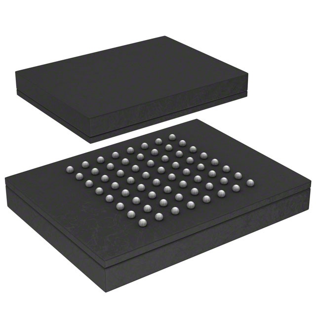
| Device Package | 54-FBGA (8x8) | Memory Format | DRAM | Technology | DRAM | ||
|---|---|---|---|---|---|---|---|
| Memory Size | 256 Mbit | Access Time | 5.4 ns | Grade | Industrial | ||
| Clock Frequency | 166 MHz | Voltage | 1.7V ~ 1.95V | Memory Type | Volatile | ||
| Operating Temperature | -40°C – 85°C | Write Cycle Time Word Page | 12 ns | Packaging | 54-FBGA | ||
| Mounting Method | Surface Mount | Memory Interface | LVCMOS | Memory Organization | 4M x 16 | ||
| Moisture Sensitivity Level | 3 | RoHS Compliance | Compliant | REACH Compliance | REACH Unknown | ||
| Qualification | JEDEC | ECCN | EAR99 | HTS Code | 8542.32.00.24 |
Overview of M52D2561616A-6BIG2F – LPSDR SDRAM 256Mbit (4M×16×4 Banks), 166MHz, 1.8V, 54‑Ball FBGA, Industrial (‑40 °C to 85 °C)
The M52D2561616A-6BIG2F is a 268,435,456‑bit mobile synchronous DRAM organized as 4 × 4,194,304 words by 16 bits. Its synchronous design allows precise cycle control with system clock timing and supports I/O transactions on every clock cycle.
With four‑bank operation, programmable burst lengths and latencies, and JEDEC qualification, this LPSDR SDRAM is intended for high‑bandwidth, high‑performance memory system applications that require industrial temperature operation and compact FBGA packaging.
Key Features
- Memory Architecture 268,435,456‑bit organization presented as 4M × 16 with four banks for concurrent bank operation and efficient access patterns.
- High‑Speed Timing Operates at up to 166 MHz with an access time of 5.4 ns and a write cycle (word/page) of 12 ns; supports CAS latency = 3.
- Flexible Burst and Latency Programmable burst lengths (1, 2, 4, 8 and full page) and burst types (sequential and interleave) for adaptable throughput and access patterns.
- Power and I/O 1.8 V nominal supply (operating range 1.7 V–1.95 V) with LVCMOS compatibility and isolated VDDQ/VSSQ for output buffer power to improve noise immunity.
- Refresh and Low‑Power Controls Auto and self‑refresh support with 64 ms refresh period (8K cycles), plus PASR (Partial Array Self Refresh) and TCSR (Temperature Compensated Self Refresh).
- Control and Masking MRS and EMRS cycles with address key programming, DQM data masking, and standard SDRAM control signals sampled on the positive clock edge.
- Package and Temperature Range 54‑ball FBGA (8 mm × 8 mm × 1 mm body, 0.8 mm ball pitch), surface‑mount package rated for industrial operation from ‑40 °C to 85 °C; JEDEC qualified and RoHS compliant.
Typical Applications
- High‑bandwidth memory subsystems — Suitable for applications that require synchronous, high data‑rate DRAM with programmable burst and latency options.
- Mobile and portable systems — Mobile SDRAM architecture supports designs where synchronous, clocked memory access is required.
- Industrial equipment — Industrial temperature rating (‑40 °C to 85 °C) makes it appropriate for embedded systems operating in harsh environments.
Unique Advantages
- Industrial temperature capability: Rated for ‑40 °C to 85 °C to support deployment in temperature‑sensitive and industrial environments.
- Synchronous, high‑data‑rate operation: Clocked design enables predictable timing and I/O transactions on every clock cycle for deterministic memory performance.
- Flexible performance tuning: Programmable burst lengths, burst types and CAS latency allow optimization for a variety of system bandwidth and latency requirements.
- Improved output noise immunity: Separate VDDQ/VSSQ supplies isolate output buffers, helping reduce noise coupling into core logic.
- Standards and compliance: JEDEC qualification and RoHS compliance provide traceable industry conformance and environmental compliance.
- Compact, surface‑mount footprint: 54‑ball FBGA (8×8 mm) delivers a small board area for dense memory integrations.
Why Choose M52D2561616A-6BIG2F?
The M52D2561616A-6BIG2F delivers a balanced combination of synchronous high‑data‑rate operation, configurable burst/latency behavior, and industrial temperature tolerance. Its four‑bank architecture and JEDEC‑compliant feature set make it a practical choice for designers building reliable, high‑bandwidth memory subsystems in compact, surface‑mount form factors.
Because the device supports programmable timing and refresh modes (including PASR and TCSR) and provides isolated output power (VDDQ), it is well suited to designs that require predictable timing, improved signal integrity on outputs, and robust operation across a wide temperature range.
Request a quote or submit an inquiry to receive pricing, availability, and lead‑time information for the M52D2561616A-6BIG2F.


Date Founded: 1998
Headquarters: Hsinchu Science Park, Hsinchu, Taiwan
Employees: 400+
Revenue: $377.8 Million
Certifications and Memberships: N/A


