
M30LW128D110ZA6
| Part Description |
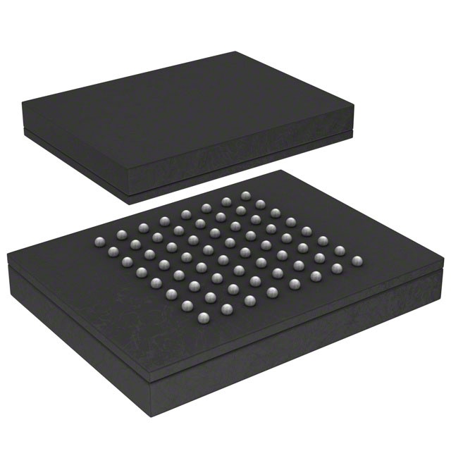
IC FLASH 128MBIT PARALLEL 64TBGA |
|---|---|
| Quantity | 42 Available (as of June 15, 2026) |
| Product Category | Memory |
|---|---|
| Manufacturer | STMicroelectronics |
| Manufacturing Status | Obsolete |
| Manufacturer Standard Lead Time | Contact Us |
| Datasheet |
Specifications & Environmental
| Device Package | 64-TBGA (10x13) | Memory Format | FLASH | Technology | FLASH | ||
|---|---|---|---|---|---|---|---|
| Memory Size | 128 Mbit | Access Time | 110 ns | Grade | Industrial | ||
| Clock Frequency | N/A | Voltage | 2.7V ~ 3.6V | Memory Type | Non-Volatile | ||
| Operating Temperature | -40°C ~ 85°C (TA) | Write Cycle Time Word Page | 110 ns | Packaging | 64-TBGA | ||
| Mounting Method | Non-Volatile | Memory Interface | Parallel | Memory Organization | 8M x 8 x 2, 4M x 16 | ||
| Moisture Sensitivity Level | 1 (Unlimited) | RoHS Compliance | RoHS non-compliant | REACH Compliance | REACH Unaffected | ||
| Qualification | N/A | ECCN | OBSOLETE | HTS Code | 8542.32.0071 |
Overview of M30LW128D110ZA6 – IC FLASH 128MBIT PARALLEL 64TBGA
The M30LW128D110ZA6 is a 128‑Mbit parallel FLASH memory device from STMicroelectronics combining two stacked 64‑Mbit FLASH dies in a single 64‑TBGA package. It provides a selectable x8 or x16 data bus and a Common Flash Interface suitable for parallel NOR Flash storage in embedded and electronic systems.
Designed for non‑volatile code and data storage, the device supports a 2.7–3.6 V supply range, VDDQ I/O buffering from 1.8 V to VDD, and an industrial operating temperature range of -40°C to 85°C to meet a variety of system integration needs.
Key Features
- Stacked memory in a single package — Two M58LW064D 64‑Mbit FLASH memories stacked to deliver 128 Mbit in a compact 64‑TBGA (10×13 mm) package.
- Flexible data bus — Wide x8 or x16 data bus selectable for byte‑ or word‑wide system interfaces to match platform requirements.
- Memory organization and capacity — 128 Mbit total organized as 8M × 8 × 2 or 4M × 16 with 128 uniform 64 KWord / 128 KByte blocks for block‑level management.
- Performance and timing — Random read access time of 110 ns; page‑mode read options (110 ns / 25 ns); 16‑word write buffer and 16 µs effective word programming time.
- Power and I/O — VDD supply range 2.7 V to 3.6 V; VDDQ for I/O buffers configurable from 1.8 V up to VDD to support multi‑voltage systems.
- Endurance and data protection — Up to 100,000 program/erase cycles per block; block protection/unprotection, 128‑bit protection register, and program/erase suspend/resume capabilities.
- Command and status features — Common Flash Interface with electronic signature (Manufacturer Code 0020h, Device Code 8817h) and status register support for program/erase monitoring.
- Package and temperature — 64‑TBGA (10×13 mm) package with operating temperature range −40°C to 85°C.
Typical Applications
- Embedded systems — Non‑volatile storage for application code and parameters where parallel x8/x16 access and 128 Mbit capacity are required.
- Industrial equipment — Firmware and lookup table storage in systems operating across −40°C to 85°C, with block protection and suspend/resume for field updates.
- Networking and communications — Storage of firmware images and configuration data benefiting from fast random reads and page‑mode access.
- Consumer and general electronics — Parallel NOR Flash for boot code and persistent data in systems using a 3 V supply domain and TBGA packaging.
Unique Advantages
- High density in a compact footprint: Two stacked 64‑Mbit devices provide 128 Mbit inside a 64‑TBGA (10×13 mm) package to save board area.
- Selectable bus width: x8 or x16 data interface lets designers match memory width to processor or bus requirements without changing the device.
- Fast access modes: 110 ns random read and page‑mode performance (110/25 ns) combined with a 16‑word write buffer speed up code fetch and programming sequences.
- Durable program/erase lifecycle: 100,000 program/erase cycles per block for robust in‑field update capability.
- Flexible I/O voltage: VDDQ support from 1.8 V to VDD enables compatibility with mixed‑voltage I/O domains.
- Block control and safety: Uniform 64 KWord blocks, a 128‑bit protection register, and suspend/resume commands enable controlled updates and protection.
Why Choose M30LW128D110ZA6?
The M30LW128D110ZA6 delivers mid‑density parallel FLASH storage with a combination of compact packaging, selectable x8/x16 I/O, and robust program/erase endurance. Its stacked‑die architecture and Common Flash Interface simplify integration where 128 Mbit of non‑volatile memory is required in a small TBGA footprint.
With industrial temperature rating, flexible VDD/VDDQ ranges, block‑level protection and suspend/resume features, this device is suited to designs that require reliable firmware and data storage and predictable programming behavior over the product life cycle. It is manufactured by STMicroelectronics and includes electronic signature and status reporting for system-level management.
If you would like pricing, lead‑time or technical ordering information for the M30LW128D110ZA6, request a quote or submit a pricing inquiry to receive details for your project.


Date Founded: 1987
Headquarters: Plan-les-Ouates, Geneva, Switzerland
Employees: 50,000+
Revenue: $17.24 Billion
Certifications and Memberships: ISO9001:2015, ISO14001:2015, ISO45001:2018, IATF16949:2016, ISO50001:2018


