MT46V16M16P-75:F
| Part Description |
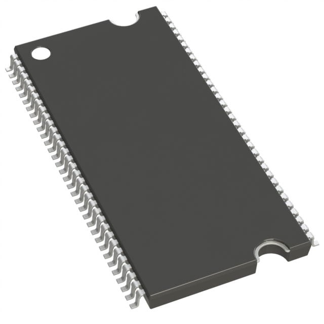
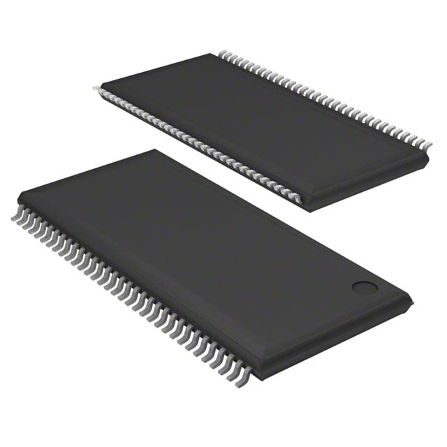
IC DRAM 256MBIT PARALLEL 66TSOP |
|---|---|
| Quantity | 727 Available (as of June 15, 2026) |

| Product Category | Memory |
|---|---|
| Manufacturer | Micron Technology Inc. |
| Manufacturing Status | Obsolete |
| Manufacturer Standard Lead Time | Contact Us |
| Datasheet |
Specifications & Environmental
| Device Package | 66-TSOP | Memory Format | DRAM | Technology | SDRAM - DDR | ||
|---|---|---|---|---|---|---|---|
| Memory Size | 256 Mbit | Access Time | 750 ps | Grade | Commercial | ||
| Clock Frequency | 133 MHz | Voltage | 2.3V ~ 2.7V | Memory Type | Volatile | ||
| Operating Temperature | 0°C ~ 70°C (TA) | Write Cycle Time Word Page | 15 ns | Packaging | 66-TSSOP (0.400", 10.16mm Width) | ||
| Mounting Method | Volatile | Memory Interface | Parallel | Memory Organization | 16M x 16 | ||
| Moisture Sensitivity Level | 2 (1 Year) | RoHS Compliance | ROHS3 Compliant | REACH Compliance | REACH Unaffected | ||
| Qualification | N/A | ECCN | EAR99 | HTS Code | 8542.32.0024 |
Overview of MT46V16M16P-75:F – IC DRAM 256Mbit Parallel 66TSOP
The MT46V16M16P-75:F is a 256 Mbit DDR SDRAM organized as 16M × 16 with a parallel memory interface. It implements a double-data-rate architecture with source-synchronous data capture and internal DLL alignment to support two data transfers per clock cycle.
Designed for board-level memory expansion where a compact 66‑TSSOP package and 2.5V-class I/O are required, the device targets systems that need predictable timing at a 133 MHz clock rate and commercial temperature operation (0°C to 70°C).
Key Features
- Core / Architecture Double Data Rate (DDR) SDRAM with internal pipelined DDR architecture providing two data accesses per clock cycle and a DLL to align DQ/DQS transitions with CK.
- Memory Organization 256 Mbit capacity organized as 16M × 16 with four internal banks for concurrent operation.
- Performance & Timing 133 MHz clock frequency (–75 timing grade), 750 ps access time, and programmable burst lengths of 2, 4, or 8 for flexible data transfer patterns.
- Data I/O and Capture Bidirectional data strobe (DQS) transmitted/received with data (x16 devices include two DQS signals, one per byte); data mask (DM) support (x16 has two DMs, one per byte).
- Interface & Signaling Differential clock inputs (CK/CK#) and 2.5V I/O (SSTL_2-compatible) signaling.
- Power Supply voltage range: 2.3 V to 2.7 V (VDD/VDDQ options documented for DDR operation).
- Refresh & Reliability Auto refresh with 8K refresh cycles and self-refresh capability documented in the device family.
- Package & Temperature 66‑TSSOP package (0.400", 10.16 mm width) specified for commercial temperature range: 0°C to +70°C.
Typical Applications
- Board-level system memory — Provides 256 Mbit of DDR memory in designs requiring a parallel DDR interface and compact TSOP packaging.
- Frame or buffer storage — Suitable for applications that require predictable burst transfers and source-synchronous data capture at 133 MHz.
- Legacy DDR interface designs — Fits systems using SSTL_2-compatible 2.5V I/O signaling and standard DDR timing grades.
Unique Advantages
- DDR source-synchronous capture: Bidirectional DQS and DLL alignment simplify timing for both reads and writes, improving data-transfer reliability.
- Byte-granular control on x16 devices: Two DQS and two DM signals (one per byte) enable finer write masking and byte-level timing control.
- Flexible burst operation: Programmable burst lengths (2, 4, 8) accommodate diverse transfer sizes and optimize bus utilization.
- Compact, board-friendly package: 66‑TSSOP package provides a narrow footprint (10.16 mm width) for space-constrained board designs.
- Commercial temperature rating: Specified 0°C to +70°C operation for standard commercial applications.
- Standard DDR signaling: 2.5V I/O (SSTL_2-compatible) and differential clock inputs simplify integration with existing DDR controllers designed for these standards.
Why Choose MT46V16M16P-75:F?
The MT46V16M16P-75:F delivers a compact 256 Mbit DDR SDRAM solution built around a 16M × 16 organization and a parallel DDR architecture that supports source-synchronous DQS capture and DLL timing alignment. Its documented timing at a 133 MHz clock rate, programmable burst lengths, and byte-level data mask support make it suitable for designs that require deterministic DDR transfers and flexible data handling.
This device is appropriate for engineers and procurement teams specifying commercial-temperature, board-mounted DDR memory in a 66‑TSSOP package where 2.5V-class I/O and standard DDR timing grades are required. Its combination of timing features, compact package, and documented refresh/self-refresh behavior supports reliable integration into a range of system designs.
Request a quote or submit a parts inquiry to obtain pricing and availability for the MT46V16M16P-75:F. Provide your quantity and required delivery timeframe to receive a prompt response.