MT46V16M16P-6T:F TR
| Part Description |
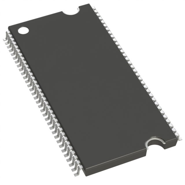
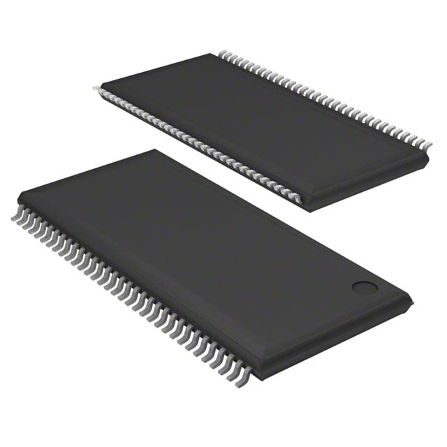
IC DRAM 256MBIT PAR 66TSOP |
|---|---|
| Quantity | 1,706 Available (as of June 15, 2026) |

| Product Category | Memory |
|---|---|
| Manufacturer | Micron Technology Inc. |
| Manufacturing Status | Obsolete |
| Manufacturer Standard Lead Time | Contact Us |
| Datasheet |
Specifications & Environmental
| Device Package | 66-TSOP | Memory Format | DRAM | Technology | SDRAM - DDR | ||
|---|---|---|---|---|---|---|---|
| Memory Size | 256 Mbit | Access Time | 700 ps | Grade | Commercial | ||
| Clock Frequency | 167 MHz | Voltage | 2.3V ~ 2.7V | Memory Type | Volatile | ||
| Operating Temperature | 0°C ~ 70°C (TA) | Write Cycle Time Word Page | 15 ns | Packaging | 66-TSSOP (0.400", 10.16mm Width) | ||
| Mounting Method | Volatile | Memory Interface | Parallel | Memory Organization | 16M x 16 | ||
| Moisture Sensitivity Level | 3 (168 Hours) | RoHS Compliance | ROHS3 Compliant | REACH Compliance | REACH Unaffected | ||
| Qualification | N/A | ECCN | EAR99 | HTS Code | 8542.32.0024 |
Overview of MT46V16M16P-6T:F TR – IC DRAM 256MBIT PAR 66TSOP
The MT46V16M16P-6T:F TR is a 256 Mbit DDR SDRAM device in a 66-TSSOP (0.400", 10.16 mm width) package, organized as 16M × 16 with four internal banks. It implements an internal pipelined double-data-rate architecture with two data accesses per clock cycle and a parallel memory interface.
Designed for applications requiring mid-density parallel DDR memory, the device supports a timing grade that enables a 167 MHz clock rate, low-voltage operation (2.3–2.7 V), and DDR features such as DLL, DQS-based source-synchronous capture, programmable burst lengths, and auto-refresh.
Key Features
- Core Architecture Double Data Rate (DDR) SDRAM with an internal pipelined DDR architecture and a DLL to align DQ/DQS transitions with CK.
- Memory Organization 256 Mbit capacity arranged as 16M × 16 with four internal banks and support for programmable burst lengths (BL = 2, 4, 8).
- Performance & Timing Supports a 167 MHz clock frequency (–6T timing grade) with an access time of 700 ps and a write cycle time (word/page) of 15 ns; data-out window for the 6T grade is specified as 2.0 ns.
- Interface & I/O Parallel memory interface with bidirectional data strobe (DQS); x16 devices include two DQS signals (one per byte) and two data mask (DM) signals. Differential clock inputs (CK/CK#) are used for timing.
- Power Nominal VDD/VDDQ of 2.5 V with an operating supply range of 2.3 V to 2.7 V; 2.5 V I/O (SSTL_2-compatible) is supported.
- System Reliability & Refresh Auto refresh and support for 8K refresh cycles (64 ms for Commercial & Industrial modes as documented); self-refresh option noted in the device family documentation (self refresh not available on AT devices).
- Package & Temperature Range 66‑pin TSSOP (66‑TSOP) package (0.400" / 10.16 mm width); commercial operating temperature 0°C to +70°C (TA).
Typical Applications
- Embedded memory systems Use as on-board parallel DDR memory where a 256 Mbit capacity and x16 data width are required in a 66‑TSSOP footprint.
- Buffering and frame storage Suitable for designs that need DDR buffering with programmable burst lengths and source-synchronous DQS timing.
- Board-level integration Provides a compact TSOP package option for legacy or space-constrained PCB layouts requiring parallel DDR SDRAM.
Unique Advantages
- Proven DDR feature set: Internal DLL, DQS source-synchronous capture, programmable burst lengths and auto-refresh simplify timing and memory control in DDR systems.
- Mid-density x16 organization: 256 Mbit (16M × 16) configuration with four internal banks enables commonly needed capacity and concurrency for moderate memory footprints.
- 66‑TSSOP package: Board-friendly TSOP footprint (0.400" / 10.16 mm) that supports compact PCB implementations and straightforward soldering processes.
- Low-voltage operation: Nominal 2.5 V operation with a supply range of 2.3–2.7 V supports low-power designs and SSTL_2-compatible I/O.
- Timing grade for 167 MHz: The –6T timing grade provides a specified data-out window and DQS–DQ skew characteristics suitable for 167 MHz clock operation.
Why Choose IC DRAM 256MBIT PAR 66TSOP?
The MT46V16M16P-6T:F TR offers a compact, mid-density DDR SDRAM solution with a standard set of DDR features—DLL alignment, DQS-based source-synchronous capture, programmable burst lengths, and auto-refresh—packaged in a 66‑TSSOP footprint. Its 16M × 16 organization, four internal banks, and –6T timing grade (supporting up to 167 MHz) make it suitable for designs that require parallel DDR memory at commercial temperatures.
With nominal 2.5 V operation (2.3–2.7 V range), specified timing windows, and a TSOP package for board-level integration, the device is well suited to engineers looking for a verifiable, standards-based DDR memory component for mid-density applications.
Request a quote or submit a pricing inquiry for the MT46V16M16P-6T:F TR to check availability and lead times.