MT46V16M16P-6T L:F TR
| Part Description |
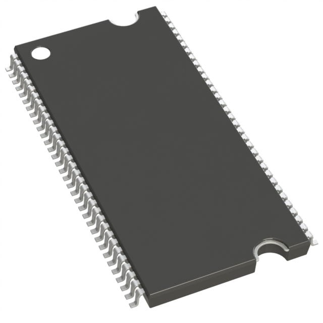
IC DRAM 256MBIT PAR 66TSOP |
|---|---|
| Quantity | 835 Available (as of June 15, 2026) |

| Product Category | DRAM Memory |
|---|---|
| Manufacturer | Micron Technology Inc. |
| Manufacturing Status | Obsolete |
| Manufacturer Standard Lead Time | Contact Us |
| Datasheet |
Specifications & Environmental
| Device Package | 66-TSOP | Memory Format | DRAM | Technology | SDRAM - DDR | ||
|---|---|---|---|---|---|---|---|
| Memory Size | 256 Mbit | Access Time | 700 ps | Grade | Commercial | ||
| Clock Frequency | 167 MHz | Voltage | 2.3V ~ 2.7V | Memory Type | Volatile | ||
| Operating Temperature | 0°C ~ 70°C (TA) | Write Cycle Time Word Page | 15 ns | Packaging | 66-TSSOP (0.400", 10.16mm Width) | ||
| Mounting Method | Volatile | Memory Interface | Parallel | Memory Organization | 16M x 16 | ||
| Moisture Sensitivity Level | 3 (168 Hours) | RoHS Compliance | ROHS3 Compliant | REACH Compliance | REACH Unaffected | ||
| Qualification | N/A | ECCN | EAR99 | HTS Code | 8542.32.0024 |
Overview of MT46V16M16P-6T L:F TR – IC DRAM 256MBIT PAR 66TSOP
The MT46V16M16P-6T L:F TR is a 256 Mbit DDR SDRAM device organized as 16M × 16 with a parallel memory interface in a 66‑TSSOP package. It implements a pipelined double‑data‑rate architecture with source‑synchronous data capture to deliver two data transfers per clock cycle.
Designed for systems requiring compact, parallel DDR memory, the device offers a 66‑pin TSOP footprint, a 2.3 V–2.7 V supply range, and commercial temperature operation (0°C to 70°C), providing a balance of density and board‑level integration.
Key Features
- Core Architecture Internal, pipelined DDR architecture delivering two data accesses per clock cycle with a DLL for timing alignment.
- Memory Organization 256 Mbit capacity configured as 16M × 16 with four internal banks for concurrent operation.
- High‑speed Operation Clock frequency specified at 167 MHz with an access time of 700 ps and a write cycle time (word/page) of 15 ns.
- Source‑synchronous I/O Bidirectional data strobe (DQS) transmitted/received with data (x16 offers two DQS lines, one per byte) for source‑synchronous data capture.
- Clock and Timing Differential clock inputs (CK, CK#), commands entered on positive CK edge, and programmable burst lengths (BL = 2, 4, or 8).
- Data Integrity and Control Data mask (DM) available for masking write data (x16 has two DMs) and support for concurrent auto precharge and tRAS lockout features.
- Refresh and Self‑Refresh Auto refresh supported with 8K refresh cycles; self refresh option documented (note: self refresh not available on AT devices per datasheet).
- Power and I/O Levels Supply voltage range 2.3 V–2.7 V; 2.5 V I/O (SSTL_2‑compatible) and separate VDD/VDDQ domains documented in the datasheet.
- Package 66‑TSSOP (0.400", 10.16 mm width) long‑lead TSOP option for board designs requiring that footprint.
- Operating Temperature Commercial temperature range 0°C to 70°C (TA).
Unique Advantages
- DDR performance per clock Pipelined DDR architecture delivering two data transfers per clock cycle improves throughput without requiring higher clock rates.
- Compact TSOP footprint 66‑TSSOP (10.16 mm width) package enables higher density on PCBs while preserving through‑board routing for parallel memory interfaces.
- Source‑synchronous capture with DQS and DLL DQS signals and an on‑chip DLL help align DQ/DQS transitions with CK for reliable timing margins in parallel DDR systems.
- Flexible memory control Programmable burst lengths and concurrent auto precharge support a range of access patterns and controller strategies.
- Robust refresh management Built‑in auto refresh with 8K cycle support simplifies system refresh requirements.
- Voltage compatibility 2.3 V–2.7 V supply range accommodates standard 2.5 V DDR system rails and VDDQ I/O signaling.
Why Choose IC DRAM 256MBIT PAR 66TSOP?
The MT46V16M16P-6T L:F TR offers a focused DDR SDRAM solution for designs that require 256 Mbit density in a 66‑pin TSOP package. Its DDR architecture, DQS/DLL timing support, and four internal banks provide deterministic, source‑synchronous operation suitable for parallel memory subsystems.
Backed by Micron Technology Inc. documentation, this device is appropriate for projects that need a defined commercial temperature range (0°C to 70°C), standard 2.5 V I/O signaling, and controlled timing grades as identified by the -6T speed option. It is suited to engineers seeking a verifiable DDR memory building block with documented timing and refresh behavior.
Request a quote or submit an inquiry to obtain pricing and availability for the MT46V16M16P-6T L:F TR. Provide your quantity and delivery requirements to receive a tailored response.