MT46V16M16P-5B:M TR
| Part Description |
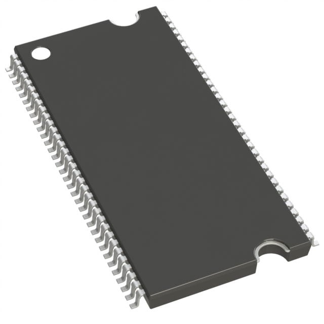
IC DRAM 256MBIT PARALLEL 66TSOP |
|---|---|
| Quantity | 1,286 Available (as of June 15, 2026) |

| Product Category | Memory |
|---|---|
| Manufacturer | Micron Technology Inc. |
| Manufacturing Status | Obsolete |
| Manufacturer Standard Lead Time | Contact Us |
| Datasheet |
Specifications & Environmental
| Device Package | 66-TSOP | Memory Format | DRAM | Technology | SDRAM - DDR | ||
|---|---|---|---|---|---|---|---|
| Memory Size | 256 Mbit | Access Time | 700 ps | Grade | Commercial | ||
| Clock Frequency | 200 MHz | Voltage | 2.5V ~ 2.7V | Memory Type | Volatile | ||
| Operating Temperature | 0°C ~ 70°C (TA) | Write Cycle Time Word Page | 15 ns | Packaging | 66-TSSOP (0.400", 10.16mm Width) | ||
| Mounting Method | Volatile | Memory Interface | Parallel | Memory Organization | 16M x 16 | ||
| Moisture Sensitivity Level | 3 (168 Hours) | RoHS Compliance | ROHS Compliant | REACH Compliance | REACH Unaffected | ||
| Qualification | N/A | ECCN | EAR99 | HTS Code | 8542.32.0036 |
Overview of MT46V16M16P-5B:M TR – IC DRAM 256MBIT PARALLEL 66TSOP
The MT46V16M16P-5B:M TR is a 256 Mbit DDR SDRAM organized as 16M x 16 with a parallel memory interface in a 66‑pin TSSOP package. It implements an internal pipelined double‑data‑rate architecture with source‑synchronous data capture for two data accesses per clock cycle.
Targeted at designs that require compact, high‑throughput volatile memory, this device delivers up to a 200 MHz clock rate (DDR mode) with 2.5 V I/O and a commercial operating temperature range. It is suited for systems that need a 16‑bit wide DDR data path in a space‑efficient TSOP footprint.
Key Features
- Core / Architecture Internal pipelined DDR architecture with a DLL to align DQ/DQS transitions and four internal banks for concurrent operation.
- Memory Organization 256 Mbit capacity organized as 16M × 16 with two DQS and two DM signals (one per byte) for the x16 configuration.
- Performance & Timing Speed grade -5B supports a 5 ns cycle time (200 MHz) at CL = 3, with an access window and data‑out window optimized for DDR operation; specified access time 700 ps and write cycle time (word page) 15 ns.
- Power & I/O VDD/VDDQ supply range 2.5 V to 2.7 V with 2.5 V I/O compatible with SSTL_2 signaling.
- Interfaces & Controls Differential clock inputs (CK/CK#), bidirectional DQS (edge‑aligned for READs, center‑aligned for WRITEs), programmable burst lengths (2, 4, 8), and data mask (DM) support for masked writes.
- Refresh & Low‑Level Functions Supports auto refresh (8K refresh cycles), and self refresh options per device variant; concurrent auto precharge and tRAS lockout supported.
- Package & Temperature 66‑pin TSSOP (0.400" / 10.16 mm width) package; specified operating temperature 0°C to 70°C (TA) for this product listing.
- Reliability & Qualification Family documentation lists AEC‑Q100 and related automotive DDR SDRAM features; product includes longer‑lead TSOP option for improved reliability and supplier quality deliverables noted in the datasheet.
Typical Applications
- Embedded systems — Provides a compact DDR memory option for microcontroller‑based designs and embedded platforms requiring a 16‑bit parallel memory interface.
- Industrial control — Fits control and instrumentation applications that need a commercial‑temperature DDR memory with predictable timing and refresh behavior.
- Networking and communications — Suitable as packet buffers or working memory where a parallel DDR interface and programmable burst lengths improve throughput.
- Legacy system upgrades — Drop‑in or redesign use where a TSOP‑packaged 16‑bit DDR SDRAM is required for board area and interface compatibility.
Unique Advantages
- DDR double‑data‑rate architecture: Two data transfers per clock cycle increase effective bandwidth while maintaining a simple parallel interface.
- 16‑bit data path in compact TSOP: 16M × 16 organization in a 66‑pin TSSOP delivers a wide data bus in a small footprint for board area‑sensitive designs.
- 200 MHz (DDR) timing: -5B speed grade supports 200 MHz clocking (CL = 3), enabling higher throughput for time‑critical applications.
- Byte‑level control: Dual DQS and DM signals for the x16 device provide byte‑wise strobe and mask control for flexible data handling.
- SSTL_2‑compatible I/O at 2.5 V: Industry‑standard 2.5 V signaling simplifies interface design where SSTL_2 levels are required.
- Qualified family features: Datasheet references AEC‑Q100 and extended TSOP options for improved reliability and supplier quality artifacts.
Why Choose MT46V16M16P-5B:M TR?
The MT46V16M16P-5B:M TR offers a balanced combination of DDR performance, 16‑bit parallel data width, and a compact 66‑pin TSSOP package for designs that need mid‑density volatile memory with predictable timing. Its -5B timing grade provides a 200 MHz DDR operating point and features such as DLL‑aligned DQS and programmable burst lengths to simplify high‑speed memory interfacing.
This device is appropriate for engineers specifying 256 Mbit DDR SDRAM in commercial temperature applications who require clear electrical and timing characteristics, a compact footprint, and documented qualification context from the datasheet and manufacturer.
If you require pricing, lead time, or want to submit a request for quote for MT46V16M16P-5B:M TR, please request a quote or submit an RFQ for availability and detailed ordering information.