MT46V16M16P-5B:M
| Part Description |
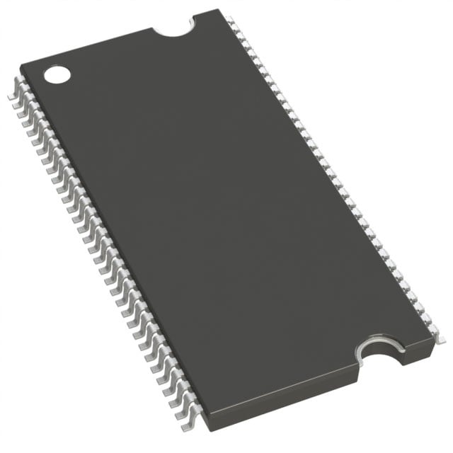
IC DRAM 256MBIT PARALLEL 66TSOP |
|---|---|
| Quantity | 890 Available (as of June 15, 2026) |

| Product Category | DRAM Memory |
|---|---|
| Manufacturer | Micron Technology Inc. |
| Manufacturing Status | Obsolete |
| Manufacturer Standard Lead Time | Contact Us |
| Datasheet |
Specifications & Environmental
| Device Package | 66-TSOP | Memory Format | DRAM | Technology | SDRAM - DDR | ||
|---|---|---|---|---|---|---|---|
| Memory Size | 256 Mbit | Access Time | 700 ps | Grade | Commercial | ||
| Clock Frequency | 200 MHz | Voltage | 2.5V ~ 2.7V | Memory Type | Volatile | ||
| Operating Temperature | 0°C ~ 70°C (TA) | Write Cycle Time Word Page | 15 ns | Packaging | 66-TSSOP (0.400", 10.16mm Width) | ||
| Mounting Method | Volatile | Memory Interface | Parallel | Memory Organization | 16M x 16 | ||
| Moisture Sensitivity Level | 3 (168 Hours) | RoHS Compliance | ROHS3 Compliant | REACH Compliance | REACH Unaffected | ||
| Qualification | N/A | ECCN | EAR99 | HTS Code | 8542.32.0024 |
Overview of MT46V16M16P-5B:M – IC DRAM 256Mbit Parallel 66-TSSOP
The MT46V16M16P-5B:M is a 256 Mbit, x16 DDR SDRAM organized as 16M × 16 with a parallel memory interface. It implements an internal, pipelined double-data-rate architecture with source‑synchronous data capture to deliver two data transfers per clock cycle.
Targeted for board-level memory applications that require a compact 66‑TSSOP package and 2.5 V I/O signaling, this device provides programmable burst lengths, on‑chip DLL and DQS support, and timing options up to 200 MHz (–5B timing grade) for higher throughput designs.
Key Features
- Core / Architecture Internal pipelined double-data-rate (DDR) architecture with bidirectional DQS for source‑synchronous capture and a DLL to align DQ/DQS with CK.
- Memory 256 Mbit total capacity arranged as 16M × 16 with four internal banks for concurrent operation and programmable burst lengths (2, 4, 8).
- Performance / Timing Timing grade –5B supports up to 200 MHz clock rate (DDR400, CL = 3); specified access window and data‑out windows per datasheet timing tables.
- Interface Parallel DDR interface with differential clock inputs (CK/CK#), two DQS strobes for x16 (one per byte), and data mask (DM) functionality for masked writes.
- Power 2.5 V nominal supply with specified operating range of 2.5 V ±0.2 V (general) and 2.6 V ±0.1 V for DDR400 conditions; VDD and VDDQ supported.
- Refresh & Self‑Maintenance Auto refresh (8K count), selectable self refresh options (note: self refresh availability varies by device option), and concurrent auto precharge support.
- Package 66‑pin TSSOP (0.400", 10.16 mm width) with longer‑lead TSOP option for improved board reliability (OCPL variant noted in datasheet).
- Operating Range & Reliability Specified commercial operating ambient temperature of 0°C to 70°C (TA). Datasheet indicates AEC‑Q100 qualification for applicable options.
- Write Cycle Word/page write cycle time specified at 15 ns.
Typical Applications
- Automotive electronic systems Datasheet includes AEC‑Q100 and automotive DDR SDRAM options; suitable for automotive memory functions where qualified device options are selected.
- Embedded system memory Parallel DDR x16 organization and source‑synchronous DQS make the device suitable as system memory for embedded and real‑time controllers that require compact board footprint.
- Board‑level memory expansion 66‑TSSOP package and 256 Mbit density provide a space‑efficient option for adding DDR memory to module and single‑board designs.
- High‑throughput interface buffering Programmable burst lengths and dual‑byte strobes support designs requiring predictable, low‑latency data transfers at DDR rates.
Unique Advantages
- DDR architecture with source‑synchronous DQS: Two data transfers per clock cycle and DQS alignment simplify high‑speed data capture and timing closure.
- Timing grade –5B (200 MHz): Enables DDR400 operation at CL = 3 for designs targeting higher throughput.
- Byte‑level strobes and masking (x16): Two DQS strobes and DM pins (one per byte) allow precise byte‑wise control for reads and writes.
- SSTL_2‑compatible 2.5 V I/O: Standard 2.5 V signaling support eases integration with SSTL_2 I/O systems.
- Qualified device options noted in datasheet: Datasheet lists AEC‑Q100 qualification and OCPL TSOP variants, providing options for enhanced reliability and automotive program support.
- Compact 66‑TSSOP package: Small footprint with longer‑lead TSOP option for improved solderability and board reliability where needed.
Why Choose MT46V16M16P-5B:M?
The MT46V16M16P-5B:M delivers a compact, parallel DDR SDRAM solution with 256 Mbit density, DDR architecture, and timing options up to 200 MHz. Its x16 organization, byte‑level strobes, programmable bursts, and SSTL_2‑compatible 2.5 V I/O make it suitable for board‑level memory applications that require predictable DDR throughput and a small TSOP footprint.
With device options and qualifications documented in the datasheet (including AEC‑Q100 where offered) and OCPL TSOP variants for improved reliability, this device is appropriate for designs that need scalable DDR performance combined with package flexibility and specified operating characteristics.
Request a quote or submit your project requirements to receive pricing and availability information for the MT46V16M16P-5B:M.