MT46V32M16CV-5B:J TR
| Part Description |
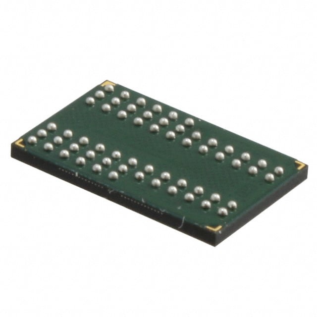
IC DRAM 512MBIT PARALLEL 60FBGA |
|---|---|
| Quantity | 1,601 Available (as of June 15, 2026) |

| Product Category | Memory |
|---|---|
| Manufacturer | Micron Technology Inc. |
| Manufacturing Status | Obsolete |
| Manufacturer Standard Lead Time | Contact Us |
| Datasheet |
Specifications & Environmental
| Device Package | 60-FBGA (8x12.5) | Memory Format | DRAM | Technology | SDRAM - DDR | ||
|---|---|---|---|---|---|---|---|
| Memory Size | 512 Mbit | Access Time | 700 ps | Grade | Commercial | ||
| Clock Frequency | 200 MHz | Voltage | 2.5V ~ 2.7V | Memory Type | Volatile | ||
| Operating Temperature | 0°C ~ 70°C (TA) | Write Cycle Time Word Page | 15 ns | Packaging | 60-TFBGA | ||
| Mounting Method | Volatile | Memory Interface | Parallel | Memory Organization | 32M x 16 | ||
| Moisture Sensitivity Level | 3 (168 Hours) | RoHS Compliance | ROHS3 Compliant | REACH Compliance | REACH Unknown | ||
| Qualification | N/A | ECCN | EAR99 | HTS Code | 8542.32.0024 |
Overview of MT46V32M16CV-5B:J TR – 512 Mbit Parallel DDR SDRAM, 60‑FBGA
The MT46V32M16CV-5B:J TR is a 512 Mbit volatile DRAM organized as 32M × 16 using DDR SDRAM architecture with a parallel memory interface. It provides synchronous double data rate operation at a 200 MHz clock frequency for systems that require parallel DDR memory capacity and predictable access timing.
Engineered for commercial-temperature applications, this device is supplied in a 60‑TFBGA / 60‑FBGA (8 × 12.5 mm) package and supports standard DDR supply voltages, making it suitable for designs that need mid-density DDR storage in a compact BGA footprint.
Key Features
- Memory Core & Organization 512 Mbit DRAM organized as 32M × 16, providing a balanced density and data width for parallel DDR memory implementations.
- DDR SDRAM Architecture Synchronous DDR operation with a specified clock frequency of 200 MHz to support double data rate transfers.
- Performance Timing Access time of 700 ps and a write cycle time (word page) of 15 ns for predictable read/write timing characteristics.
- Supply Voltage Operates from 2.5 V to 2.7 V, matching standard DDR voltage requirements for compatible system power domains.
- Package Available in a 60‑TFBGA (60‑FBGA, 8 × 12.5 mm) package for compact board-level integration and BGA mounting.
- Operating Temperature Specified for commercial temperature operation from 0°C to 70°C (TA).
- Interface Parallel memory interface suitable for systems designed around parallel DDR memory architectures.
Typical Applications
- Embedded systems Provides on-board DDR storage for buffering and temporary data storage in embedded designs requiring 512 Mbit capacity.
- Consumer electronics Used where compact BGA packaging and DDR performance are required within commercial-temperature consumer products.
- System memory modules Suitable for incorporation into memory subsystems or modules that utilize parallel DDR SDRAM banks.
Unique Advantages
- Moderate density DDR memory: 512 Mbit capacity (32M × 16) offers a mid-range storage option for designs that need more than small SRAM/DRAM but less than high-density parts.
- Predictable timing: 700 ps access time and 15 ns write cycle time provide deterministic timing characteristics for system designers managing memory timing budgets.
- Standard DDR voltage: Operation at 2.5–2.7 V aligns with common DDR supply rails, simplifying power-domain planning.
- Compact BGA footprint: 60‑TFBGA / 60‑FBGA (8 × 12.5 mm) package enables high-density board integration while maintaining a recognizable package outline for assembly.
- Commercial temperature rating: Specified 0°C to 70°C operating range for designs targeting commercial-environment deployments.
- Parallel DDR interface: Parallel memory interface supports established DDR system architectures and memory controller implementations.
Why Choose IC DRAM 512MBIT PARALLEL 60FBGA?
The MT46V32M16CV-5B:J TR positions itself as a practical mid-density DDR SDRAM option for designs that require 512 Mbit of volatile storage with synchronous DDR operation and compact BGA packaging. Its combination of 200 MHz clock operation, defined access and write timings, and 2.5–2.7 V supply requirements makes it suitable for systems built around parallel DDR memory banks.
This device is well suited to engineers designing commercial-temperature electronics that need predictable DDR timing, a moderate density footprint, and a 60‑FBGA form factor for board-level integration.
If you need pricing, lead-time or availability information, request a quote or submit an inquiry to discuss requirements and get a formal quote from our team.