MT48LC16M16A2B4-7E:G
| Part Description |
IC DRAM 256MBIT PAR 54VFBGA |
|---|---|
| Quantity | 1,013 Available (as of June 18, 2026) |
| Product Category | DRAM Memory |
|---|---|
| Manufacturer | Micron Technology Inc. |
| Manufacturing Status | Obsolete |
| Manufacturer Standard Lead Time | Contact Us |
| Datasheet |
Specifications & Environmental
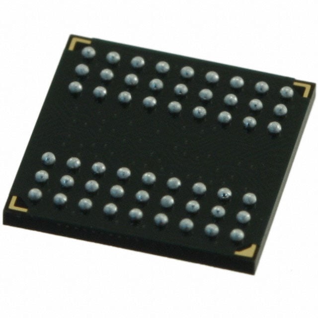
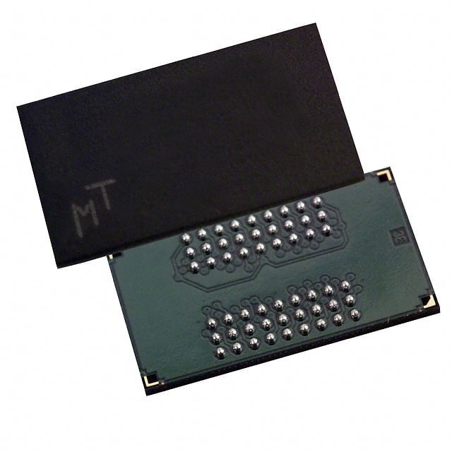
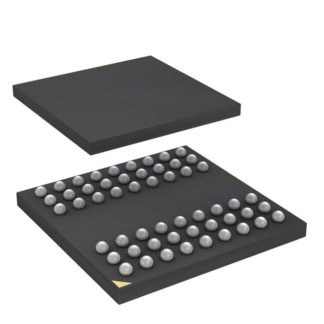
| Device Package | 54-VFBGA (8x8) | Memory Format | DRAM | Technology | SDRAM | ||
|---|---|---|---|---|---|---|---|
| Memory Size | 256 Mbit | Access Time | 5.4 ns | Grade | Commercial | ||
| Clock Frequency | 133 MHz | Voltage | 3V ~ 3.6V | Memory Type | Volatile | ||
| Operating Temperature | 0°C ~ 70°C (TA) | Write Cycle Time Word Page | 14 ns | Packaging | 54-VFBGA | ||
| Mounting Method | Volatile | Memory Interface | Parallel | Memory Organization | 16M x 16 | ||
| Moisture Sensitivity Level | 3 (168 Hours) | RoHS Compliance | ROHS3 Compliant | REACH Compliance | REACH Unaffected | ||
| Qualification | N/A | ECCN | EAR99 | HTS Code | 8542.32.0024 |
Overview of MT48LC16M16A2B4-7E:G – IC DRAM 256MBIT PAR 54VFBGA
The MT48LC16M16A2B4-7E:G is a 256 Mbit synchronous DRAM device organized as 16M × 16 with a parallel memory interface. It implements fully synchronous SDRAM architecture with registered inputs and internal, pipelined operation suitable for designs requiring PC100/PC133-class SDRAM behavior.
Key value comes from its 133 MHz clock capability, programmable burst operation and internal bank structure for efficient row/column handling, all delivered in a compact 54-ball VFBGA (8×8) package for space-constrained boards operating in commercial temperature ranges.
Key Features
- SDR SDRAM core Fully synchronous operation with all signals registered on the positive edge of the system clock and internal, pipelined operation allowing column address changes every clock cycle.
- Memory organization 256 Mbit capacity organized as 16M × 16 with 4 internal banks for improved access efficiency and hidden row access/precharge.
- Speed and timing Clock frequency 133 MHz; part number -7E corresponds to 133 MHz with 2-2-2 timing (RCD-RP-CL) per datasheet. Listed access time: 5.4 ns.
- Programmable burst and refresh Supports programmable burst lengths (1, 2, 4, 8, or full page), auto precharge, auto refresh and self-refresh modes (self-refresh not available on AT devices as noted in the datasheet).
- Interface compatibility LVTTL-compatible inputs and outputs and a parallel memory interface suitable for PC100/PC133-compliant designs.
- Power Single-supply operation specified from 3.0 V to 3.6 V (3.3 V ±0.3 V typical per datasheet).
- Package and mounting 54-ball VFBGA package (8 mm × 8 mm) in a compact footprint for space-optimized PCB layouts.
- Operating temperature Commercial temperature range: 0°C to 70°C (TA).
Typical Applications
- PC100/PC133-compatible systems — Use where PC100 or PC133-compliant SDRAM timing and 133 MHz clock operation are required.
- Synchronous memory subsystems — For systems that require fully synchronous DRAM with pipelined operation and internal bank management to improve throughput.
- Space-constrained designs — Compact 54-ball VFBGA (8×8) package for boards with limited real estate.
Unique Advantages
- Direct PC100/PC133 alignment: The device supports PC100 and PC133 compliance options and 133 MHz operation which simplifies integration into legacy synchronous memory designs.
- Pipelined, banked architecture: Internal banks and pipelined operation allow column address changes every clock cycle, improving effective data throughput for burst transfers.
- Flexible burst and refresh options: Programmable burst lengths and multiple refresh modes (auto refresh and self-refresh) provide design flexibility for power and performance trade-offs.
- Straightforward power interface: Single 3.0–3.6 V supply range aligns with common 3.3 V system rails, easing power-supply design.
- Compact BGA package: 54-ball VFBGA (8×8) enables smaller board footprint while maintaining parallel SDRAM connectivity.
Why Choose IC DRAM 256MBIT PAR 54VFBGA?
The MT48LC16M16A2B4-7E:G delivers a balanced combination of synchronous SDRAM performance, predictable timing (133 MHz, -7E timing), and a compact package for designs that require a 256 Mbit parallel DRAM solution. Its internal bank architecture, programmable burst lengths and standard refresh modes make it suitable for applications that need deterministic, clock-synchronous memory behavior.
This device is well suited for commercial-temperature systems that demand PC100/PC133-class SDRAM characteristics, a 3.3 V single-supply interface, and a small 54-ball VFBGA footprint for board-level space savings.
Request a quote or submit an RFQ to obtain pricing and availability for the MT48LC16M16A2B4-7E:G for your design and production planning.