MT48LC16M16A2BG-75:D
| Part Description |
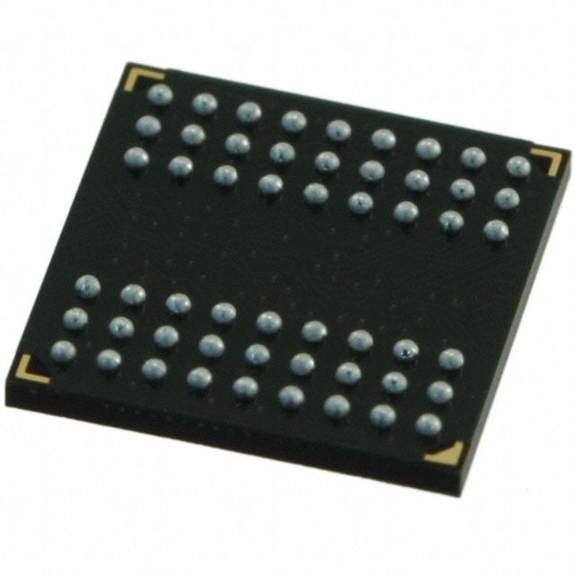
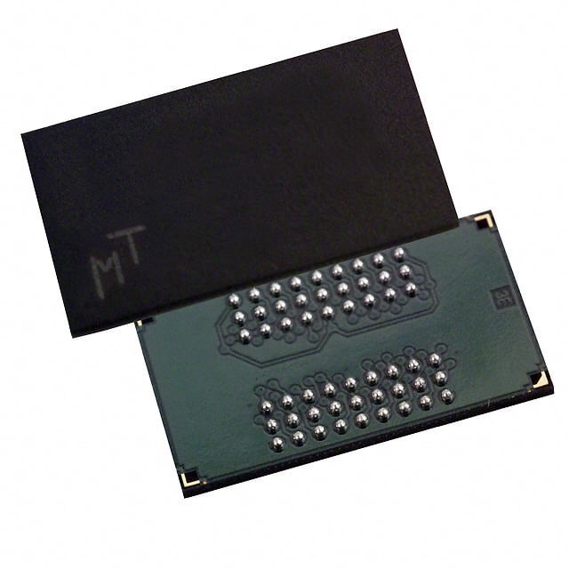
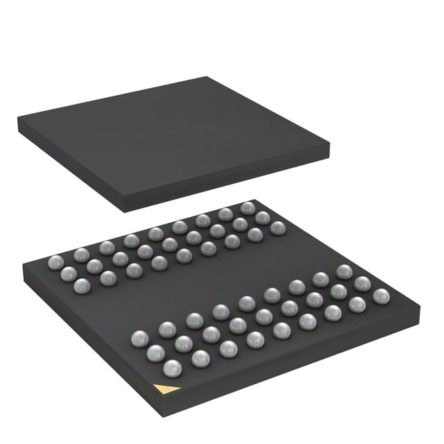
IC DRAM 256MBIT PAR 54VFBGA |
|---|---|
| Quantity | 927 Available (as of June 18, 2026) |

| Product Category | DRAM Memory |
|---|---|
| Manufacturer | Micron Technology Inc. |
| Manufacturing Status | Obsolete |
| Manufacturer Standard Lead Time | Contact Us |
| Datasheet |
Specifications & Environmental
| Device Package | 54-VFBGA (8x14) | Memory Format | DRAM | Technology | SDRAM | ||
|---|---|---|---|---|---|---|---|
| Memory Size | 256 Mbit | Access Time | 5.4 ns | Grade | Commercial | ||
| Clock Frequency | 133 MHz | Voltage | 3V ~ 3.6V | Memory Type | Volatile | ||
| Operating Temperature | 0°C ~ 70°C (TA) | Write Cycle Time Word Page | 15 ns | Packaging | 54-VFBGA | ||
| Mounting Method | Volatile | Memory Interface | Parallel | Memory Organization | 16M x 16 | ||
| Moisture Sensitivity Level | 2 (1 Year) | RoHS Compliance | ROHS3 Compliant | REACH Compliance | REACH Unaffected | ||
| Qualification | N/A | ECCN | EAR99 | HTS Code | 8542.32.0024 |
Overview of MT48LC16M16A2BG-75:D – IC DRAM 256MBIT PAR 54VFBGA
The MT48LC16M16A2BG-75:D is a 256 Mbit volatile SDRAM organized as 16M × 16 with a parallel memory interface in a 54-ball VFBGA (8×14) package. It is a fully synchronous SDR SDRAM device with internal pipelined operation and internal banks designed for high-throughput, burst-oriented memory access.
Designed for systems targeting PC100/PC133 timing, the device operates at a clock frequency of 133 MHz, supports programmable burst lengths and auto refresh/self refresh modes, and requires a 3.0 V to 3.6 V supply over a commercial temperature range of 0 °C to 70 °C.
Key Features
- Core Architecture SDR SDRAM, fully synchronous with all signals registered on the positive edge of the system clock and internal, pipelined operation for column changes every clock cycle.
- Memory Organization 256 Mbit total capacity organized as 16M × 16 with four internal banks (4 Meg × 16 × 4 banks), enabling burst and banked operations.
- Performance & Timing Clock frequency 133 MHz (PC133-compliant), access time 5.4 ns, and write cycle time (word page) of 15 ns; timing options include target RCD‑RP‑CL of 3‑3‑3 at the -75 speed grade.
- Data Transfer Modes Programmable burst lengths (1, 2, 4, 8, or full page), auto precharge, concurrent auto precharge and auto refresh modes, and self refresh support.
- Interface & I/O Parallel memory interface with LVTTL‑compatible inputs and outputs for standard synchronous signaling.
- Power Single supply operation in the range 3.0 V to 3.6 V (datasheet specifies single 3.3 V ±0.3 V operation).
- Package & Temperature 54‑ball VFBGA package (8×14 mm footprint) with commercial operating temperature range 0 °C to 70 °C (TA).
- Standards Compliance PC100- and PC133-compliant timing grades are specified in the device family documentation.
Typical Applications
- PC100/PC133 memory subsystems Use where PC100/PC133 timing compliance is required for synchronous DRAM operation.
- Embedded systems High-density parallel SDRAM for embedded controllers and platforms that require burst transfers and banked memory access.
- Buffering and frame storage Parallel SDRAM organization and programmable burst lengths suitable for buffering, temporary data storage, or frame buffers in digital systems.
Unique Advantages
- Synchronous, pipelined operation: All signals registered on the positive clock edge and internal pipelining allow predictable, clock-aligned data transfers.
- Flexible burst control: Programmable burst lengths (1, 2, 4, 8, full page) support a range of host transfer strategies and throughput requirements.
- Banked memory architecture: Four internal banks hide row access/precharge timing and enable more efficient continuous data access patterns.
- Industry timing grades: PC100/PC133 timing options provide defined RCD/RP/CL targets for system timing design.
- Compact BGA footprint: 54‑ball VFBGA (8×14 mm) package supports higher board density and compact system layouts.
- Standard commercial temperature and supply: 0 °C to 70 °C operating range and 3.0 V–3.6 V supply align with common commercial embedded designs.
Why Choose IC DRAM 256MBIT PAR 54VFBGA?
The MT48LC16M16A2BG-75:D provides a synchronous, banked SDRAM solution with PC100/PC133 timing options, a 16M × 16 organization, and programmable burst modes suited for systems requiring predictable, clock-aligned memory transfers. Its 54-ball VFBGA package enables compact board integration while offering the timing and refresh features needed for burst-oriented designs.
This device is appropriate for engineers specifying a 256 Mbit parallel SDRAM from Micron Technology Inc. for commercial-temperature embedded platforms, buffering, or subsystem memory where PC100/PC133 timing and standard 3.3 V supply operation are required.
Request a quote or contact sales to obtain pricing, lead time, and availability for MT48LC16M16A2BG-75:D. Provide part number and required quantities to receive a formal quote.