MT48LC16M16A2TG-75:D TR
| Part Description |
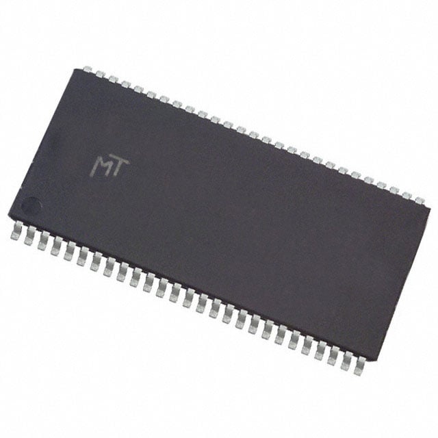
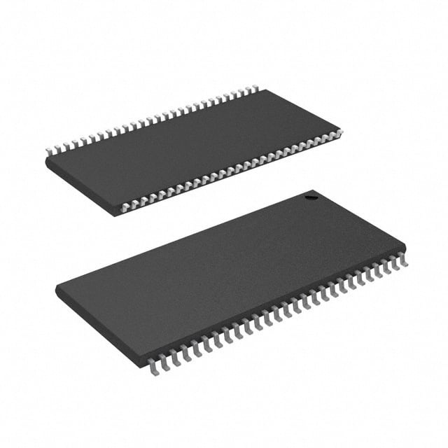
IC DRAM 256MBIT PAR 54TSOP II |
|---|---|
| Quantity | 220 Available (as of June 15, 2026) |

| Product Category | Memory |
|---|---|
| Manufacturer | Micron Technology Inc. |
| Manufacturing Status | Obsolete |
| Manufacturer Standard Lead Time | Contact Us |
| Datasheet |
Specifications & Environmental
| Device Package | 54-TSOP II | Memory Format | DRAM | Technology | SDRAM | ||
|---|---|---|---|---|---|---|---|
| Memory Size | 256 Mbit | Access Time | 5.4 ns | Grade | Commercial | ||
| Clock Frequency | 133 MHz | Voltage | 3V ~ 3.6V | Memory Type | Volatile | ||
| Operating Temperature | 0°C ~ 70°C (TA) | Write Cycle Time Word Page | 15 ns | Packaging | 54-TSOP (0.400", 10.16mm Width) | ||
| Mounting Method | Volatile | Memory Interface | Parallel | Memory Organization | 16M x 16 | ||
| Moisture Sensitivity Level | 3 (168 Hours) | RoHS Compliance | N/A | REACH Compliance | REACH Unaffected | ||
| Qualification | N/A | ECCN | EAR99 | HTS Code | 8542.32.0024 |
Overview of MT48LC16M16A2TG-75:D TR – IC DRAM 256MBIT PAR 54TSOP II
The MT48LC16M16A2TG-75:D TR is a 256 Mbit synchronous DRAM organized as 16M × 16 with a parallel memory interface. It implements SDR SDRAM architecture with fully synchronous operation and is offered in a 54‑pin TSOP II (0.400", 10.16 mm width) package.
Designed for systems requiring PC100/PC133‑compliant SDR SDRAM, this device delivers 133 MHz clock operation, internal pipelined bank architecture and programmable burst lengths to support high‑throughput, synchronous memory designs.
Key Features
- Memory Core 256 Mbit SDRAM organized as 16M × 16 with 4 internal banks; parallel DRAM format for conventional SDRAM memory architectures.
- Performance PC133‑compliant operation with a clock frequency of 133 MHz and an access time of 5.4 ns; internal pipelined operation and registered inputs on the positive clock edge enable column address changes every cycle.
- Burst and Command Flexibility Programmable burst lengths (1, 2, 4, 8 or full page), auto precharge, auto refresh and concurrent auto precharge/auto refresh modes support flexible data transfer patterns.
- Refresh and Retention Supports auto refresh and self refresh (self refresh not available on AT devices) with 8K refresh cycles and documented commercial refresh timing.
- Timing and Cycle Characteristics Write cycle time (word/page) specified at 15 ns; timing options include -75 speed grade (133 MHz) with corresponding RCD/RP/CL targets noted in the datasheet.
- Power Single supply operation at 3.3 V nominal with an allowed range of 3.0 V to 3.6 V (3.3 V ±0.3 V).
- Package and Temperature Supplied in a 54‑pin TSOP II (0.400", 10.16 mm width) plastic package; commercial operating temperature range 0°C to +70°C (TA).
- I/O Levels LVTTL‑compatible inputs and outputs as specified in the product documentation.
Typical Applications
- PC100/PC133 system memory Where PC100 or PC133‑compliant SDR SDRAM is required, this device provides a 256 Mbit solution in a standard TSOP II footprint.
- Parallel SDRAM memory expansion 16M × 16 organization and 4 internal banks enable implementation of 256 Mbit memory arrays for conventional SDRAM designs.
- Board designs with TSOP II footprint The 54‑pin TSOP II (0.400") package supports compact board layouts requiring this standard package size.
Unique Advantages
- Standards‑aligned timing: PC100 and PC133 compliance provides defined timing targets for system designers and matching platform requirements.
- Synchronous, pipelined operation: Registered inputs and internal pipelining allow column addresses to change every clock cycle, supporting predictable synchronous operation.
- Flexible burst modes and auto management: Programmable burst lengths plus auto precharge/auto refresh modes simplify controller design for varied access patterns.
- Compact TSOP II packaging: 54‑pin TSOP II (0.400", 10.16 mm) package offers a standard, space‑efficient footprint for board integration.
- Wide supply tolerance: Operation across 3.0 V to 3.6 V accommodates nominal 3.3 V systems with ±0.3 V margin.
Why Choose MT48LC16M16A2TG-75:D TR?
The MT48LC16M16A2TG-75:D TR delivers a documented PC100/PC133‑compliant SDR SDRAM solution in a 256 Mbit density, combining synchronous, pipelined operation with programmable burst behavior and standard TSOP II packaging. Its electrical and timing specifications—including 133 MHz clock capability, 5.4 ns access time, and 3.0–3.6 V supply range—are provided for straightforward integration into systems that require conventional SDRAM memory.
Backed by Micron Technology Inc., the device is suitable for designers needing a verified SDRAM building block with defined refresh behavior, LVTTL‑compatible I/O and a commercial temperature range of 0°C to +70°C.
If you need pricing or availability for MT48LC16M16A2TG-75:D TR, request a quote or submit a pricing inquiry and our team will respond with current lead times and ordering options.