MT48LC16M16A2TG-7E:D TR
| Part Description |
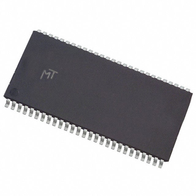
IC DRAM 256MBIT PAR 54TSOP II |
|---|---|
| Quantity | 1,824 Available (as of June 15, 2026) |

| Product Category | Memory |
|---|---|
| Manufacturer | Micron Technology Inc. |
| Manufacturing Status | Obsolete |
| Manufacturer Standard Lead Time | Contact Us |
| Datasheet |
Specifications & Environmental
| Device Package | 54-TSOP II | Memory Format | DRAM | Technology | SDRAM | ||
|---|---|---|---|---|---|---|---|
| Memory Size | 256 Mbit | Access Time | 5.4 ns | Grade | Commercial | ||
| Clock Frequency | 133 MHz | Voltage | 3V ~ 3.6V | Memory Type | Volatile | ||
| Operating Temperature | 0°C ~ 70°C (TA) | Write Cycle Time Word Page | 14 ns | Packaging | 54-TSOP (0.400", 10.16mm Width) | ||
| Mounting Method | Volatile | Memory Interface | Parallel | Memory Organization | 16M x 16 | ||
| Moisture Sensitivity Level | 3 (168 Hours) | RoHS Compliance | RoHS non-compliant | REACH Compliance | REACH Unaffected | ||
| Qualification | N/A | ECCN | EAR99 | HTS Code | 8542.32.0024 |
Overview of MT48LC16M16A2TG-7E:D TR – IC DRAM 256MBIT PAR 54TSOP II
The MT48LC16M16A2TG-7E:D TR is a 256 Mbit synchronous DRAM organized as 16M × 16 with a parallel memory interface in a 54‑pin TSOP II package. It implements SDR SDRAM architecture with internal banks, pipelined operation and PC100/PC133 compliance for systems targeting synchronous DRAM operation at 133 MHz.
Designed for systems requiring a 3.3 V single-supply parallel SDRAM device with programmable burst modes and standard SDRAM control features, this device delivers predictable timing and a compact package for space-constrained board designs.
Key Features
- SDR SDRAM Core Fully synchronous SDRAM with all signals registered on the positive edge of the system clock and internal pipelined operation allowing column address changes every clock cycle.
- Memory Organization & Capacity 256 Mbit capacity organized as 16M × 16 with 4 internal banks for concurrent row access/precharge management.
- Performance & Timing PC100- and PC133-compliant; specified clock frequency 133 MHz for the -7E speed grade. Datasheet timing for -7E indicates a 2-2-2 RCD-RP-CL target (CL = 15 ns).
- Low-level Access Access time listed at 5.4 ns and write cycle time (word/page) of 14 ns for tight read/write control.
- Burst & Refresh Modes Programmable burst lengths (1, 2, 4, 8, full page), auto precharge, auto refresh and self-refresh support as described in the device specification.
- Electrical & I/O Single-supply operation at 3.0 V to 3.6 V (datasheet references 3.3 V ±0.3 V) with LVTTL-compatible inputs and outputs.
- Package & Temperature Supplied in a 54‑pin TSOP II (0.400", 10.16 mm width) plastic package; commercial operating temperature range 0°C to +70°C.
Typical Applications
- Systems requiring PC100/PC133-compliant SDRAM — Use where synchronous 133 MHz SDRAM timing and compatibility are required.
- Parallel SDRAM memory expansion — 256 Mbit capacity in a 16M × 16 organization for designs needing parallel DRAM resources.
- Compact board designs — 54‑pin TSOP II package supports space-constrained applications that require standard TSOP footprints.
Unique Advantages
- Standards-based performance: PC100/PC133 compliance and a defined -7E speed grade provide predictable timing for system integration.
- Flexible data access: Programmable burst lengths and internal bank architecture improve throughput and simplify burst-oriented transfers.
- Single-supply simplicity: 3.0 V–3.6 V operation (3.3 V nominal) reduces supply rail complexity for systems using legacy 3.3 V designs.
- Compact package: 54‑pin TSOP II (400 mil) package enables higher board density while maintaining a standard footprint.
- Commercial temperature suitability: Rated for 0°C to +70°C operation to match typical commercial electronics environments.
Why Choose IC DRAM 256MBIT PAR 54TSOP II?
The MT48LC16M16A2TG-7E:D TR provides a standards-based SDR SDRAM solution in a compact 54‑pin TSOP II package, combining a 256 Mbit capacity with PC100/PC133 timing and internal banked architecture for efficient burst transfers. Its 3.0 V–3.6 V single-supply operation, LVTTL I/O compatibility and commercial temperature rating make it suitable for designs that require predictable SDRAM behavior and a familiar TSOP footprint.
This device is well suited to engineers and procurement teams integrating parallel SDRAM into systems where known timing, burst control and board-space considerations are key factors in memory selection.
Request a quote or submit a pricing and availability inquiry to discuss volume pricing, lead times and ordering options for the MT48LC16M16A2TG-7E:D TR.