MT48LC2M32B2B5-6A AIT:J
| Part Description |
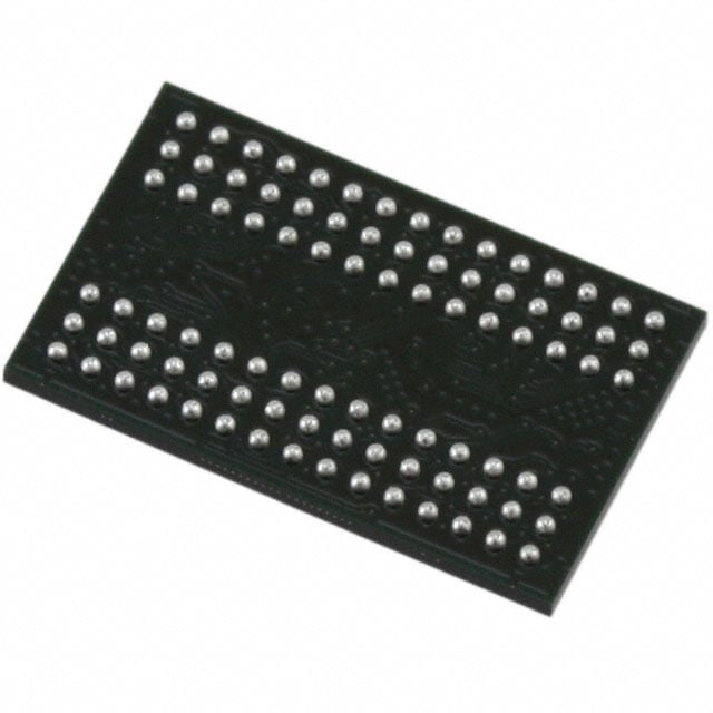
IC DRAM 64MBIT PAR 90VFBGA |
|---|---|
| Quantity | 600 Available (as of June 14, 2026) |

| Product Category | Memory |
|---|---|
| Manufacturer | Micron Technology Inc. |
| Manufacturing Status | Active |
| Manufacturer Standard Lead Time | 28 Weeks |
| Datasheet |
Specifications & Environmental
| Device Package | 90-VFBGA (8x13) | Memory Format | DRAM | Technology | SDRAM | ||
|---|---|---|---|---|---|---|---|
| Memory Size | 64 Mbit | Access Time | 5.4 ns | Grade | Automotive | ||
| Clock Frequency | 167 MHz | Voltage | 3V ~ 3.6V | Memory Type | Volatile | ||
| Operating Temperature | -40°C ~ 85°C (TA) | Write Cycle Time Word Page | 12 ns | Packaging | 90-VFBGA | ||
| Mounting Method | Volatile | Memory Interface | Parallel | Memory Organization | 2M x 32 | ||
| Moisture Sensitivity Level | 3 (168 Hours) | RoHS Compliance | ROHS3 Compliant | REACH Compliance | REACH Unaffected | ||
| Qualification | AEC-Q100 | ECCN | EAR99 | HTS Code | 8542.32.0002 |
Overview of MT48LC2M32B2B5-6A AIT:J – IC DRAM 64MBIT PAR 90VFBGA
The MT48LC2M32B2B5-6A AIT:J is a 64 Mbit, parallel-interface SDR SDRAM organized as 2M × 32. It provides fully synchronous DRAM operation in a compact 90-ball VFBGA (8×13 mm) package and is offered as an AEC-Q100 qualified device for automotive-grade applications.
Designed for embedded systems that need deterministic synchronous memory, this device delivers 167 MHz clock operation with low access latency and programmable burst/timing options to match a range of system timing requirements.
Key Features
- Core Memory Organization — 64 Mbit density in a 2M × 32 configuration (512K × 32 × 4 banks) for predictable row/column addressing and banked operation.
- SDR SDRAM Architecture — Fully synchronous operation with all signals registered on the positive clock edge, internal pipelined operation, and internal banks to hide row access/precharge.
- Programmable Burst & Timing — Programmable burst lengths (1, 2, 4, 8, full page) and support for CAS latency options (CL = 1, 2, 3) to tune throughput and latency.
- Performance — Target clock frequency 167 MHz with a specified access time of 5.4 ns and a word/page write cycle time of 12 ns.
- Power & I/O — Single-supply operation at 3.0 V to 3.6 V (3.3 V ±0.3 V) with LVTTL-compatible inputs and outputs and a parallel memory interface.
- Package & Mounting — 90-ball VFBGA (90-VFBGA, 8×13 mm) package for compact board-level integration.
- Reliability & Temperature — AEC-Q100 qualification and an operating ambient temperature range of −40 °C to +85 °C (TA).
Typical Applications
- Automotive Electronics — Use in automotive ECUs and modules where AEC-Q100 qualification and −40 °C to +85 °C operation are required.
- Embedded Control Systems — Local working memory and buffering for microcontroller- or DSP-based control applications using a parallel SDRAM interface.
- Communications and Networking — Packet buffering and temporary data storage in systems that leverage synchronous, banked DRAM operation.
Unique Advantages
- Automotive-qualified component: AEC-Q100 qualification aligns the device with automotive reliability requirements for system designers.
- Pipelined, banked architecture: Internal pipelining and multiple banks allow column-address changes each clock and help hide row access/precharge latencies.
- Flexible timing control: Multiple CAS latency and burst length options let designers trade latency and throughput to match system timing.
- Compact VFBGA footprint: The 90-ball VFBGA (8×13 mm) package supports dense PCB layouts while providing full SDRAM functionality.
- Single-supply compatibility: Operation from 3.0 V to 3.6 V (3.3 V nominal) simplifies power-rail design in legacy and modern 3.3 V systems.
Why Choose IC DRAM 64MBIT PAR 90VFBGA?
This MT48LC2M32B2B5-6A AIT:J SDRAM balances compact packaging, automotive-grade qualification, and flexible synchronous SDRAM features to support embedded and automotive designs that require predictable memory timing and a small board footprint. Its 2M × 32 organization, banked architecture, and programmable burst/timing modes deliver configurability for a range of buffering and working-memory roles.
The combination of AEC-Q100 qualification, 3.0–3.6 V single-supply operation, and a 90-ball VFBGA package makes this device suitable for designers focused on long-term robustness, space-constrained layouts, and systems that require a standardized SDR SDRAM interface.
Request a quote or submit an inquiry to confirm pricing, availability, and lead times for the MT48LC2M32B2B5-6A AIT:J.