MT48LC2M32B2B5-6A:J TR
| Part Description |
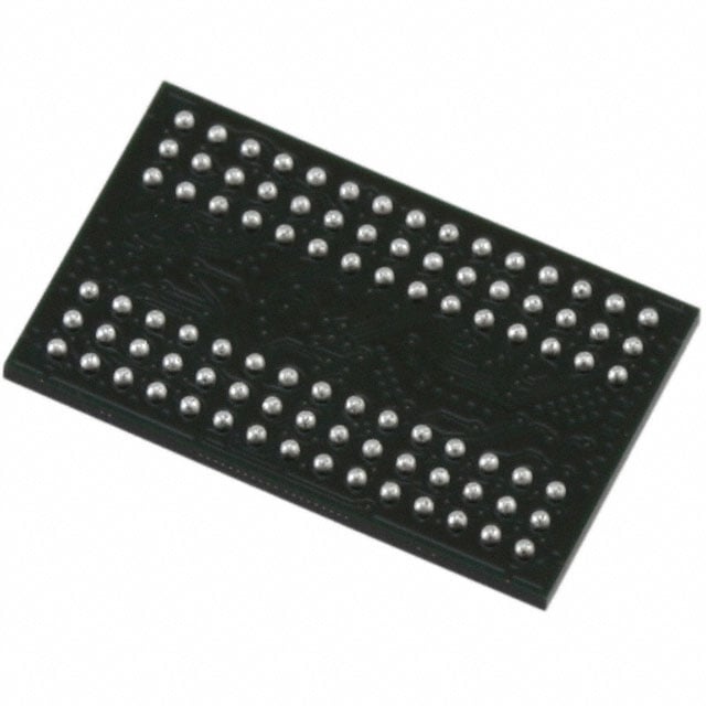
IC DRAM 64MBIT PAR 90VFBGA |
|---|---|
| Quantity | 1,531 Available (as of June 15, 2026) |

| Product Category | Memory |
|---|---|
| Manufacturer | Micron Technology Inc. |
| Manufacturing Status | Obsolete |
| Manufacturer Standard Lead Time | Contact Us |
| Datasheet |
Specifications & Environmental
| Device Package | 90-VFBGA (8x13) | Memory Format | DRAM | Technology | SDRAM | ||
|---|---|---|---|---|---|---|---|
| Memory Size | 64 Mbit | Access Time | 5.4 ns | Grade | Commercial | ||
| Clock Frequency | 167 MHz | Voltage | 3V ~ 3.6V | Memory Type | Volatile | ||
| Operating Temperature | 0°C ~ 70°C (TA) | Write Cycle Time Word Page | 12 ns | Packaging | 90-VFBGA | ||
| Mounting Method | Volatile | Memory Interface | Parallel | Memory Organization | 2M x 32 | ||
| Moisture Sensitivity Level | 3 (168 Hours) | RoHS Compliance | ROHS3 Compliant | REACH Compliance | REACH Unaffected | ||
| Qualification | N/A | ECCN | EAR99 | HTS Code | 8542.32.0002 |
Overview of MT48LC2M32B2B5-6A:J TR – IC DRAM 64Mbit PAR 90VFBGA
The MT48LC2M32B2B5-6A:J TR is a 64 Mbit SDR SDRAM organized as 2M × 32 with internal bank architecture (512K × 32 × 4 banks). It implements a fully synchronous parallel SDRAM interface optimized for systems that require standard PC100-class SDRAM timing and predictable burst access.
Key value propositions include synchronous pipelined operation with programmable burst lengths and support for multiple CAS latencies, delivered in a compact 90-ball VFBGA package with a 3.0 V to 3.6 V supply and commercial operating range (0 °C to 70 °C).
Key Features
- SDR SDRAM core — Fully synchronous operation with all signals registered on the positive clock edge for deterministic timing and pipelined column accesses.
- Memory organization — 2M × 32 configuration (512K × 32 × 4 banks) providing a total of 64 Mbit of DRAM storage.
- Performance — Clock frequency 167 MHz and an access time specification of 5.4 ns; timing options and speed grades available for various cycle-time requirements.
- Programmable burst and latency — Supports programmable burst lengths (1, 2, 4, 8, or full page) and CAS latency options (CL = 1, 2, 3) to match system throughput and latency needs.
- Refresh and power modes — Auto refresh and self-refresh support for retained data during low-activity intervals; 4096-cycle refresh architecture described in the datasheet.
- Interface and signaling — Parallel memory interface with LVTTL-compatible inputs and outputs for standard system-level integration.
- Power and timing — Single-supply operation from 3.0 V to 3.6 V with write cycle time (word/page) specified at 12 ns.
- Package — 90-ball VFBGA (8 mm × 13 mm) package; datasheet lists a 90-ball VFBGA Pb-free option.
- Operating temperature — Commercial ambient range of 0 °C to 70 °C (TA).
Typical Applications
- System memory for legacy and embedded platforms — Acts as parallel SDRAM storage where 64 Mbit capacity and standard PC100-class timing are required.
- Buffered frame or data storage — Useful for designs that need burstable parallel read/write windows with programmable burst lengths.
- General-purpose SDRAM expansion — Fits systems requiring a compact VFBGA form factor and conventional 3.3 V supply operation.
Unique Advantages
- Standard synchronous architecture: Fully synchronous SDRAM design enables predictable, clocked operation and simple timing integration with existing parallel memory controllers.
- Flexible timing options: Support for multiple CAS latencies and programmable burst lengths allows tuning for latency-sensitive or high-throughput modes.
- Compact VFBGA footprint: 90-ball VFBGA (8 × 13 mm) reduces board area compared with larger packages while maintaining a robust ball-grid connection.
- Wide supply tolerance: Operates across a 3.0 V to 3.6 V range to accommodate common 3.3 V system rails and supply variation.
- Refresh and low-power features: Auto refresh and self-refresh modes described in the datasheet help preserve data during idle periods and simplify power management.
- PC100-class compatibility: Documented PC100 compliance and standard signaling simplify integration into legacy systems designed around PC100 timing.
Why Choose IC DRAM 64MBIT PAR 90VFBGA?
The MT48LC2M32B2B5-6A:J TR positions itself as a straightforward parallel SDRAM option where established PC100-class timing, a 64 Mbit capacity, and predictable synchronous operation are required. Its combination of programmable burst lengths, multiple CAS latency support, and internal bank architecture provides designers with flexible performance tuning for embedded and system-level memory needs.
This device is appropriate for designs that need a compact VFBGA package and standard 3.3 V supply compatibility, offering a balance of integration and timing control backed by detailed datasheet specifications for timing, refresh, and power modes.
Request a quote or submit a sales inquiry for the MT48LC2M32B2B5-6A:J TR to get pricing, availability, and ordering information tailored to your project requirements.