MT48LC2M32B2P-5:G
| Part Description |
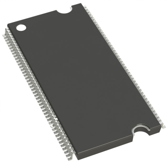
IC DRAM 64MBIT PAR 86TSOP II |
|---|---|
| Quantity | 338 Available (as of June 18, 2026) |

| Product Category | DRAM Memory |
|---|---|
| Manufacturer | Micron Technology Inc. |
| Manufacturing Status | Obsolete |
| Manufacturer Standard Lead Time | Contact Us |
| Datasheet |
Specifications & Environmental
| Device Package | 86-TSOP II | Memory Format | DRAM | Technology | SDRAM | ||
|---|---|---|---|---|---|---|---|
| Memory Size | 64 Mbit | Access Time | 4.5 ns | Grade | Commercial | ||
| Clock Frequency | 200 MHz | Voltage | 3V ~ 3.6V | Memory Type | Volatile | ||
| Operating Temperature | 0°C ~ 70°C (TA) | Write Cycle Time Word Page | N/A | Packaging | 86-TFSOP (0.400", 10.16mm Width) | ||
| Mounting Method | Volatile | Memory Interface | Parallel | Memory Organization | 2M x 32 | ||
| Moisture Sensitivity Level | 2 (1 Year) | RoHS Compliance | ROHS Compliant | REACH Compliance | REACH Unaffected | ||
| Qualification | N/A | ECCN | EAR99 | HTS Code | 8542.32.0002 |
Overview of MT48LC2M32B2P-5:G – IC DRAM 64MBIT PAR 86TSOP II
The MT48LC2M32B2P-5:G is a 64 Mbit SDR SDRAM organized as 2M × 32 with a parallel memory interface in an 86-pin TSOP II package. It implements a fully synchronous SDRAM architecture with internal banks and pipelined operation for predictable, clocked memory access.
Designed for commercial-temperature applications (0°C to 70°C), the device targets systems requiring PC100-class SDRAM behavior with a 200 MHz clock option, flexible burst lengths and selectable CAS latency settings.
Key Features
- SDR SDRAM Architecture Fully synchronous device with all signals registered on the positive edge of the system clock and internal pipelined operation for column-address changes every cycle.
- Memory Organization & Density 2M × 32 configuration (512K × 32 × 4 banks) delivering 64 Mbit of DRAM in a single package.
- Timing & Performance 200 MHz clock frequency (–5 speed grade) with access timing examples including 4.5 ns access time and support for CAS latencies (CL) of 1, 2 and 3; programmable burst lengths of 1, 2, 4, 8 or full page.
- Refresh & Power Modes Auto refresh and self-refresh support (self-refresh not available on AT devices), with 4K refresh cycles and standard refresh intervals as defined in the device documentation.
- Interface & I/O Parallel memory interface with LVTTL-compatible inputs and outputs for standard 3.3 V signaling.
- Supply & Temperature Single 3.3 V ±0.3 V supply range (3.0 V to 3.6 V) and commercial operating temperature range of 0°C to 70°C.
- Package 86-pin TSOP II (400 mil / 10.16 mm width) standard package for compact board integration.
Typical Applications
- PC100-class systems — Memory subsystem implementations and legacy platforms requiring PC100-compliant SDRAM timing and behavior.
- Embedded systems — Local DRAM for embedded controllers and modules that require a 64 Mbit parallel SDRAM with 3.3 V operation.
- Consumer electronics — Buffer and working memory in consumer devices designed to operate within the commercial temperature range and standard 86-TSOP II footprint.
Unique Advantages
- PC100 timing compatibility: Offers a 200 MHz (–5) speed grade option and timing parameters aligned with PC100-class SDRAM requirements for predictable system integration.
- Flexible latency and burst control: Programmable CAS latencies (1–3) and burst lengths (1, 2, 4, 8, full page) let designers tune access patterns for application needs.
- Compact, industry-standard packaging: 86-pin TSOP II package simplifies board layout for designs constrained by PCB area while maintaining standard pinout conventions.
- Standard 3.3 V operation: 3.0 V to 3.6 V supply range ensures compatibility with common 3.3 V system power rails.
- Banked, pipelined architecture: Internal banks and pipelined operation help hide row access/precharge overhead and support efficient, continuous column accesses.
Why Choose IC DRAM 64MBIT PAR 86TSOP II?
The MT48LC2M32B2P-5:G provides a compact, commercially rated SDR SDRAM option that combines standard 86-TSOP II packaging with PC100-class timing and flexible latency/burst controls. It is suitable for designs that require a 64 Mbit parallel SDRAM device operating from a 3.3 V supply within a 0°C to 70°C range.
Choose this device for system-level designs that need an established SDRAM feature set—programmable burst lengths, multiple CAS latencies, internal banking and standard electrical interfaces—delivered in a footprint compatible with common board layouts.
Request a quote or submit a pricing inquiry for MT48LC2M32B2P-5:G to evaluate integration into your next design or to obtain production and availability information.