MT48LC2M32B2P-5:G TR
| Part Description |
IC DRAM 64MBIT PAR 86TSOP II |
|---|---|
| Quantity | 1,049 Available (as of June 15, 2026) |

| Product Category | DRAM Memory |
|---|---|
| Manufacturer | Micron Technology Inc. |
| Manufacturing Status | Obsolete |
| Manufacturer Standard Lead Time | Contact Us |
| Datasheet |
Specifications & Environmental
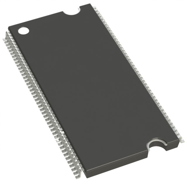
| Device Package | 86-TSOP II | Memory Format | DRAM | Technology | SDRAM | ||
|---|---|---|---|---|---|---|---|
| Memory Size | 64 Mbit | Access Time | 4.5 ns | Grade | Commercial | ||
| Clock Frequency | 200 MHz | Voltage | 3V ~ 3.6V | Memory Type | Volatile | ||
| Operating Temperature | 0°C ~ 70°C (TA) | Write Cycle Time Word Page | N/A | Packaging | 86-TFSOP (0.400", 10.16mm Width) | ||
| Mounting Method | Volatile | Memory Interface | Parallel | Memory Organization | 2M x 32 | ||
| Moisture Sensitivity Level | 2 (1 Year) | RoHS Compliance | ROHS3 Compliant | REACH Compliance | REACH Unaffected | ||
| Qualification | N/A | ECCN | EAR99 | HTS Code | 8542.32.0002 |
Overview of MT48LC2M32B2P-5:G TR – IC DRAM 64MBIT PAR 86TSOP II
The MT48LC2M32B2P-5:G TR is a 64 Mbit, x32 SDR SDRAM device from Micron Technology. It implements a 2M × 32 memory organization with four internal banks and a parallel memory interface in an 86-pin TSOP II package.
Designed for systems requiring synchronous, pipelined DRAM with configurable burst lengths and standard timing options, this device provides 200 MHz clock operation, a single 3.3 V supply range, and commercial temperature operation for board-level memory subsystems.
Key Features
- Memory Architecture — 64 Mbit capacity organized as 2M × 32 (512K × 32 × 4 banks) to support banked access and internal row/column addressing.
- SDR SDRAM Core — Fully synchronous operation with all signals registered on the positive edge of the system clock and internal pipelined operation for column address changes every clock cycle.
- Performance — Speed grade -5 supports a 200 MHz clock (5 ns cycle time) with an access time listed as 4.5 ns in the product specification.
- Programmable Burst & Latency — Programmable burst lengths of 1, 2, 4, 8, or full page and support for CAS latencies (CL) of 1, 2, and 3.
- Refresh & Power Modes — Auto refresh and self-refresh modes are supported, with 64 ms/4096-cycle refresh for commercial operation; note self-refresh availability exceptions noted in device options.
- Signal & Power — LVTTL-compatible inputs and outputs; single 3.3 V ±0.3 V power supply (3.0 V to 3.6 V specified).
- Package — 86-pin TSOP II (0.400", 10.16 mm width) standard package (86-TFSOP), suitable for board-level mounting.
- Operating Range — Commercial temperature range: 0°C to +70°C (TA).
Typical Applications
- PC100-compliant systems — Use in systems targeting PC100 timing and compatibility, leveraging the device’s PC100-compliant speed grade.
- Parallel SDRAM memory subsystems — Board-level memory replacement or integration where a 64 Mbit, x32 parallel SDRAM in an 86-pin TSOP II package is required.
- Designs requiring 3.3 V single-supply operation — Applications needing a single 3.3 V ±0.3 V supply and LVTTL-compatible I/O.
- Commercial-temperature equipment — Systems operating within 0°C to +70°C seeking a standard SDRAM component with auto-refresh and self-refresh features.
Unique Advantages
- Banked memory organization: Four internal banks (512K × 32 × 4) enable hidden row access/precharge and improve access flexibility.
- Flexible burst and latency options: Programmable burst lengths and CAS latencies (1, 2, 3) allow tuning for system timing and throughput requirements.
- High-frequency operation: Support for 200 MHz clocking (speed grade -5) provides deterministic synchronous timing for pipelined memory designs.
- Standard package footprint: 86-pin TSOP II (400 mil) packaging facilitates board-level integration and replacement in existing TSOP II footprints.
- Standardized signaling and power: LVTTL-compatible I/O and a single 3.3 V ±0.3 V supply simplify interface and power rail design.
- Integrated refresh functionality: Auto refresh and self-refresh modes reduce external refresh management overhead in system designs.
Why Choose MT48LC2M32B2P-5:G TR?
The MT48LC2M32B2P-5:G TR combines a standard SDR SDRAM architecture with a compact 86-pin TSOP II package and industry-standard signaling to meet board-level memory requirements. Its 2M × 32 organization, four internal banks, and programmable burst/latency settings provide design flexibility for synchronous, pipelined memory subsystems operating from a single 3.3 V supply.
This Micron SDRAM device is suited to commercial-temperature designs that require predictable PC100-class timing and integrated refresh modes. The device’s package and electrical specifications make it appropriate for engineers specifying or replacing parallel SDRAM components in existing TSOP II footprints.
Request a quote or submit a parts inquiry to obtain pricing, availability, and ordering information for the MT48LC2M32B2P-5:G TR.