MT48LC2M32B2P-55:G
| Part Description |
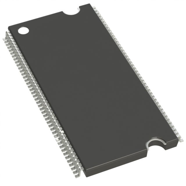
IC DRAM 64MBIT PAR 86TSOP II |
|---|---|
| Quantity | 1,477 Available (as of June 15, 2026) |

| Product Category | Memory |
|---|---|
| Manufacturer | Micron Technology Inc. |
| Manufacturing Status | Obsolete |
| Manufacturer Standard Lead Time | Contact Us |
| Datasheet |
Specifications & Environmental
| Device Package | 86-TSOP II | Memory Format | DRAM | Technology | SDRAM | ||
|---|---|---|---|---|---|---|---|
| Memory Size | 64 Mbit | Access Time | 5 ns | Grade | Commercial | ||
| Clock Frequency | 183 MHz | Voltage | 3V ~ 3.6V | Memory Type | Volatile | ||
| Operating Temperature | 0°C ~ 70°C (TA) | Write Cycle Time Word Page | N/A | Packaging | 86-TFSOP (0.400", 10.16mm Width) | ||
| Mounting Method | Volatile | Memory Interface | Parallel | Memory Organization | 2M x 32 | ||
| Moisture Sensitivity Level | 2 (1 Year) | RoHS Compliance | ROHS3 Compliant | REACH Compliance | REACH Unaffected | ||
| Qualification | N/A | ECCN | EAR99 | HTS Code | 8542.32.0002 |
Overview of MT48LC2M32B2P-55:G – IC DRAM 64MBIT PAR 86TSOP II
The MT48LC2M32B2P-55:G is a 64 Mbit, x32 SDR SDRAM device from Micron Technology, Inc. It implements a 2M × 32 memory organization with four internal banks and a parallel memory interface for synchronous system memory applications.
Designed for commercial temperature operation (0°C to +70°C), the device targets PC100-class and legacy systems that require a 3.3 V single-supply SDRAM in an 86-pin TSOP II (400 mil) package.
Key Features
- Memory Organization — 64 Mbit (2M × 32) configuration implemented as 512K × 32 × 4 banks, providing banked operation for hidden row access and precharge.
- SDR SDRAM Core — Fully synchronous SDR SDRAM with internal pipelined operation; column address can be changed every clock cycle and programmable burst lengths of 1, 2, 4, 8, or full page.
- Performance (‑55 Speed Grade) — Target clock frequency of 183 MHz for the -55 speed grade with timing of RCD-RP-CL = 3-3-3 (RCD = 16.5 ns, RP = 16.5 ns, CL = 16.5 ns).
- Refresh and Power Modes — Supports auto refresh and self-refresh modes (note: self-refresh not available on AT devices) and 4K refresh count; single 3.3 V ±0.3 V supply (3.0–3.6 V).
- Interface and Signaling — Parallel memory interface with LVTTL-compatible inputs and outputs for straightforward system integration.
- Package and Temperature — 86-pin TSOP II (400 mil, 10.16 mm width) plastic package suitable for surface-mount assembly; commercial operating range 0°C to +70°C.
Typical Applications
- PC100-class and legacy computing systems — Provides synchronous DRAM memory for designs requiring PC100-compliant SDRAM performance and timing.
- Embedded commercial systems — 64 Mbit density and TSOP II footprint for embedded boards operating within 0°C to +70°C.
- Memory expansion for existing platforms — Drop-in 86-pin TSOP II form factor for systems using x32 SDRAM devices and parallel interfaces.
Unique Advantages
- Banked architecture for throughput: Four internal banks hide row access/precharge and enable efficient pipelined operation for continuous column access.
- Flexible burst control: Programmable burst lengths (1, 2, 4, 8, full page) allow designers to match transfer behavior to system requirements.
- PC100 compliance and defined timing: -55 speed grade specifies 183 MHz operation with RCD/RP/CL = 3-3-3, enabling predictable timing for system designers.
- Industry-standard signaling and supply: LVTTL-compatible I/O and a single 3.3 V ±0.3 V supply simplify interface and power-supply design.
- Compact, assembly-ready package: 86-pin TSOP II (400 mil) offers a space-efficient, surface-mount solution for board-level memory implementation.
Why Choose MT48LC2M32B2P-55:G?
The MT48LC2M32B2P-55:G combines a standard x32 SDR SDRAM architecture with defined PC100-class timing and a compact 86-pin TSOP II package, making it suitable for commercial embedded and legacy computing designs that need a 64 Mbit synchronous DRAM. Its banked internal structure, programmable burst lengths and LVTTL-compatible interface deliver predictable, easy-to-integrate memory behavior.
This device is appropriate for designers seeking a commercially rated SDRAM with clear timing parameters (183 MHz, RCD/RP/CL = 16.5 ns for the -55 grade), a single 3.3 V supply window, and a surface-mount TSOP II footprint for board-level implementation.
If you would like pricing, lead-time information, or a formal quote for MT48LC2M32B2P-55:G, please request a quote or contact sales with your requirements and quantity.