
MT48LC2M32B2P-6 IT:G
| Part Description |
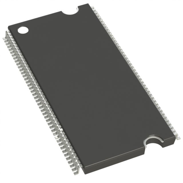
IC DRAM 64MBIT PAR 86TSOP II |
|---|---|
| Quantity | 601 Available (as of June 15, 2026) |
| Product Category | Memory |
|---|---|
| Manufacturer | Micron Technology Inc. |
| Manufacturing Status | Obsolete |
| Manufacturer Standard Lead Time | Contact Us |
| Datasheet |
Specifications & Environmental
| Device Package | 86-TSOP II | Memory Format | DRAM | Technology | SDRAM | ||
|---|---|---|---|---|---|---|---|
| Memory Size | 64 Mbit | Access Time | 5.5 ns | Grade | Industrial | ||
| Clock Frequency | 167 MHz | Voltage | 3V ~ 3.6V | Memory Type | Volatile | ||
| Operating Temperature | -40°C ~ 85°C (TA) | Write Cycle Time Word Page | 12 ns | Packaging | 86-TFSOP (0.400", 10.16mm Width) | ||
| Mounting Method | Volatile | Memory Interface | Parallel | Memory Organization | 2M x 32 | ||
| Moisture Sensitivity Level | 2 (1 Year) | RoHS Compliance | ROHS3 Compliant | REACH Compliance | REACH Unaffected | ||
| Qualification | N/A | ECCN | EAR99 | HTS Code | 8542.32.0002 |
Overview of MT48LC2M32B2P-6 IT:G – IC DRAM 64MBIT PAR 86TSOP II
The MT48LC2M32B2P-6 IT:G is a 64Mbit (2M × 32) SDR SDRAM organized for parallel memory interfaces in an 86-pin TSOP II package. It provides fully synchronous operation with internal pipelined architecture and internal banks to improve access efficiency for systems that require standard SDRAM performance.
Targeted for designs needing a compact 64Mbit parallel DRAM, this device offers PC100-compliant synchronous operation, selectable burst lengths, and a 3.3V-class supply with an industrial operating temperature range of −40°C to 85°C.
Key Features
- SDR SDRAM core Fully synchronous SDR SDRAM architecture with registered signals on the positive clock edge.
- Memory organization 2M × 32 organization delivering 64 Mbit capacity suitable for parallel memory mapping.
- Performance and timing 167 MHz clock frequency (speed grade -6), 5.5 ns access time, and write cycle time (word/page) of 12 ns for predictable timing performance.
- Internal banking and pipelining Internal 4-bank architecture and pipelined operation allow column address changes every clock cycle and hide row access/precharge latencies.
- Programmable burst and CAS Programmable burst lengths (1, 2, 4, 8, or full page) and support for CAS latencies of 1, 2, and 3.
- Refresh and power modes Auto refresh and self-refresh support with 4096-cycle refresh; includes auto precharge and concurrent auto precharge/auto refresh modes.
- Interface and I/O Parallel memory interface with LVTTL-compatible inputs and outputs.
- Power and temperature Single 3.3V ±0.3V supply range (3.0V–3.6V) and industrial operating temperature range of −40°C to +85°C (TA).
- Package 86-pin TSOP II (400 mil) package, 86-TFSOP footprint with 10.16 mm width for compact board-level integration.
Typical Applications
- Parallel SDRAM systems For designs that require a 64Mbit parallel SDRAM organized as 2M × 32 with an 86-pin TSOP II footprint.
- Buffering and data staging Programmable burst lengths and internal banking make this device suitable for buffering and temporary data storage in synchronous systems.
- Industrial equipment The −40°C to +85°C operating range supports use in industrial temperature environments.
- PC100-class synchronous designs PC100-compliant operation and synchronous timing make it applicable where legacy PC100-class SDRAM behavior is required.
Unique Advantages
- Compact TSOP II footprint: 86-pin TSOP II (400 mil) package with a 10.16 mm width enables dense board layouts while maintaining parallel interface accessibility.
- Flexible timing and burst control: Programmable burst lengths and support for multiple CAS latencies allow tuning for throughput and latency trade-offs.
- Internal banks and pipelining: Four internal banks and pipelined operation reduce effective access latency by enabling column address changes every clock cycle.
- Robust operating conditions: Single 3.3V-class power supply and industrial temperature range (−40°C to +85°C) support a wide range of operating environments.
- Synchronous, PC100-compliant operation: Registered signals on the positive clock edge and PC100 compliance simplify integration into synchronous memory subsystems.
Why Choose IC DRAM 64MBIT PAR 86TSOP II?
The MT48LC2M32B2P-6 IT:G balances a compact TSOP II package with synchronous SDRAM performance and flexible timing features, making it a practical choice for systems that require a 64Mbit parallel DRAM with predictable timing and refresh behavior. Its internal banking, programmable bursts, and LVTTL-compatible I/O simplify memory subsystem design where a parallel SDRAM interface is required.
This device is suitable for engineers and procurement teams specifying 2M × 32 SDRAM for industrial-temperature designs that need a 3.3V supply class and documented timing options. Backed by Micron’s device documentation, the part provides verifiable electrical and timing specifications for deterministic integration.
Request a quote or submit an inquiry to obtain pricing, lead time, and availability for part number MT48LC2M32B2P-6 IT:G.


