MT48LC2M32B2P-5:J TR
| Part Description |
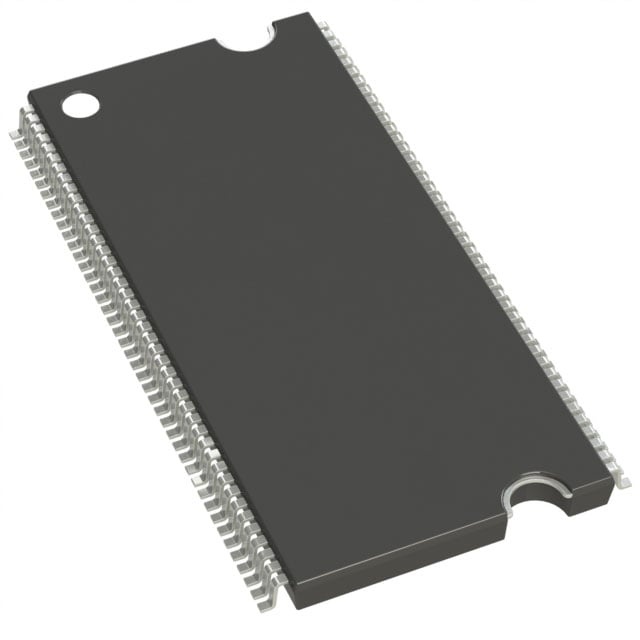
IC DRAM 64MBIT PAR 86TSOP II |
|---|---|
| Quantity | 631 Available (as of June 12, 2026) |

| Product Category | Memory |
|---|---|
| Manufacturer | Micron Technology Inc. |
| Manufacturing Status | Obsolete |
| Manufacturer Standard Lead Time | Contact Us |
| Datasheet |
Specifications & Environmental
| Device Package | 86-TSOP II | Memory Format | DRAM | Technology | SDRAM | ||
|---|---|---|---|---|---|---|---|
| Memory Size | 64 Mbit | Access Time | 4.5 ns | Grade | Commercial | ||
| Clock Frequency | 200 MHz | Voltage | 3V ~ 3.6V | Memory Type | Volatile | ||
| Operating Temperature | 0°C ~ 70°C (TA) | Write Cycle Time Word Page | N/A | Packaging | 86-TFSOP (0.400", 10.16mm Width) | ||
| Mounting Method | Volatile | Memory Interface | Parallel | Memory Organization | 2M x 32 | ||
| Moisture Sensitivity Level | 3 (168 Hours) | RoHS Compliance | ROHS3 Compliant | REACH Compliance | REACH Unaffected | ||
| Qualification | N/A | ECCN | EAR99 | HTS Code | 8542.32.0002 |
Overview of MT48LC2M32B2P-5:J TR – IC DRAM 64MBIT PAR 86TSOP II
The MT48LC2M32B2P-5:J TR is a 64 Mbit (2M × 32) SDR SDRAM offered in an 86-pin TSOP II package. It is a fully synchronous, parallel DRAM designed for systems that require PC100-compliant SDRAM functionality with programmable burst operation and internal bank architecture.
Built for 3.3 V single-supply operation and a commercial temperature range of 0 °C to 70 °C, this device targets designs where a compact 86‑TSOP II memory solution with up to 200 MHz clock operation is required.
Key Features
- Memory Architecture 2M × 32 organization delivering 64 Mbit of SDRAM in a 512K × 32 × 4 banks configuration.
- SDR SDRAM Core Fully synchronous operation with all signals registered on the positive edge of the system clock and internal pipelined operation for column-address changes every clock cycle.
- Performance Options Available with a 200 MHz clock frequency (-5 speed grade) and support for CAS latencies (CL) of 1, 2, and 3. Specified access time: 4.5 ns.
- Burst and Refresh Programmable burst lengths of 1, 2, 4, 8 or full page, plus auto refresh and self-refresh capability (self-refresh not available on AT devices); 4096-cycle refresh options documented in the datasheet.
- Signal Compatibility LVTTL-compatible inputs and outputs for standard parallel SDRAM interfacing.
- Power Single-supply operation at 3.3 V ±0.3 V (3.0 V to 3.6 V specified).
- Package 86-pin TSOP II (400 mil / 10.16 mm width) standard package for compact board-level mounting.
- Commercial Temperature Range Operating ambient temperature specified from 0 °C to 70 °C (TA).
Typical Applications
- PC100-compliant systems Use in systems requiring PC100-compliant SDRAM timing and behaviour at the listed speed grades.
- Embedded systems with parallel SDRAM Compact 86‑TSOP II package and 3.3 V single-supply operation make it suitable for board-level parallel memory implementations.
- Designs requiring programmable burst memory Programmable burst lengths and internal bank architecture support designs that benefit from flexible burst read/write operations.
Unique Advantages
- Fully synchronous design All signals registered on the clock edge, enabling deterministic timing behavior as specified in the datasheet.
- Flexible performance grades Multiple timing grades (including -5 at 200 MHz) and CAS latency options allow selection of the timing that matches system requirements.
- Compact TSOP II footprint 86-pin TSOP II (400 mil) package provides a space-efficient solution for board-level memory integration.
- Standard 3.3 V supply Single 3.3 V ±0.3 V supply simplifies power-domain design where 3.3 V DDR/legacy signaling is used.
- Built-in refresh and bank architecture Internal banks and auto-refresh/self-refresh modes reduce external refresh management overhead as described in the datasheet.
Why Choose MT48LC2M32B2P-5:J TR?
The MT48LC2M32B2P-5:J TR positions itself as a straightforward, standards-based SDRAM device for designs that need a 64 Mbit, x32 parallel memory solution in an 86‑TSOP II package. With PC100 compliance, programmable burst lengths, and support for multiple CAS latency settings, it is suited to systems that require synchronous DRAM timing and compact board-level packaging.
This device is appropriate for engineers specifying commercial-temperature SDRAM with a 3.3 V single-supply requirement and who need the documented timing grades and refresh behavior available in the product datasheet.
Request a quote or submit an inquiry to receive pricing, lead-time and availability details for the MT48LC2M32B2P-5:J TR.