MT48LC2M32B2P-6:G
| Part Description |
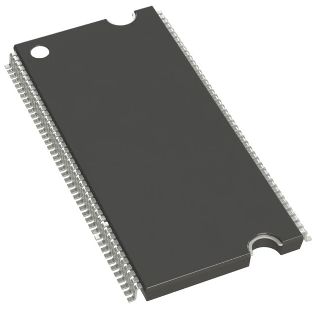
IC DRAM 64MBIT PAR 86TSOP II |
|---|---|
| Quantity | 645 Available (as of June 15, 2026) |

| Product Category | Memory |
|---|---|
| Manufacturer | Micron Technology Inc. |
| Manufacturing Status | Obsolete |
| Manufacturer Standard Lead Time | Contact Us |
| Datasheet |
Specifications & Environmental
| Device Package | 86-TSOP II | Memory Format | DRAM | Technology | SDRAM | ||
|---|---|---|---|---|---|---|---|
| Memory Size | 64 Mbit | Access Time | 5.5 ns | Grade | Commercial | ||
| Clock Frequency | 167 MHz | Voltage | 3V ~ 3.6V | Memory Type | Volatile | ||
| Operating Temperature | 0°C ~ 70°C (TA) | Write Cycle Time Word Page | 12 ns | Packaging | 86-TFSOP (0.400", 10.16mm Width) | ||
| Mounting Method | Volatile | Memory Interface | Parallel | Memory Organization | 2M x 32 | ||
| Moisture Sensitivity Level | 3 (168 Hours) | RoHS Compliance | ROHS3 Compliant | REACH Compliance | REACH Unaffected | ||
| Qualification | N/A | ECCN | EAR99 | HTS Code | 8542.32.0002 |
Overview of MT48LC2M32B2P-6:G – IC DRAM 64MBIT PAR 86TSOP II
The MT48LC2M32B2P-6:G is a 64 Mbit SDR SDRAM organized as 2M × 32 with a parallel memory interface. It implements a fully synchronous SDRAM architecture with internal banks and programmable burst lengths for flexible data transfer patterns.
This device is supplied in an 86-pin TSOP II (400 mil, 10.16 mm width) package, operates from a single 3.3 V ±0.3 V supply (specified 3.0 V to 3.6 V), and is specified for commercial temperature operation (0 °C to 70 °C). It targets designs requiring parallel SDRAM memory in a compact package with standard SDRAM feature sets.
Key Features
- Memory Architecture 64 Mbit organized as 2M × 32 with 4 internal banks (512K × 32 × 4 banks) for bank-managed row access and precharge.
- SDR SDRAM Core Fully synchronous operation with all signals registered on the positive clock edge; supports programmable burst lengths of 1, 2, 4, 8, or full page and auto precharge modes.
- Timing and Performance Specified clock frequency of 167 MHz and an access time of 5.5 ns; supports CAS latencies 1, 2, and 3 and a write cycle time (word/page) of 12 ns.
- Refresh and Power Modes Auto refresh and self-refresh modes are supported; refresh count is 4K cycles as described in the device architecture.
- Voltage and I/O Single-supply operation at 3.0 V to 3.6 V (3.3 V ±0.3 V) with LVTTL-compatible inputs and outputs documented in the device specification.
- Package and Temperature 86-pin TSOP II (400 mil) plastic package; commercial operating temperature range 0 °C to 70 °C is specified for this part number.
- Standards and Compatibility PC100-compliant implementation as documented in the device feature set and timing tables.
Typical Applications
- Legacy and parallel-memory systems Designed for systems that require a parallel SDRAM interface in a compact 86-pin TSOP II footprint.
- Buffering and frame storage Suitable for designs that need 64 Mbit of volatile SDRAM for buffering or temporary data storage using programmable burst transfers.
- Embedded platforms with standard SDRAM Fits embedded designs that leverage PC100-compatible SDRAM features and standard CAS/burst timing control.
Unique Advantages
- Compact TSOP II package: Enables space-constrained board layouts with an industry-standard 86-pin TSOP II (400 mil) form factor.
- Flexible burst and latency control: Programmable burst lengths and support for CAS latencies 1–3 allow tuning of transfer behavior to match system timing needs.
- Internal bank architecture: Four internal banks allow row access and precharge hiding to improve sustained data throughput in pipelined operation.
- Single 3.3 V supply: Standardized 3.0 V–3.6 V supply simplifies power rail requirements for systems designed around 3.3 V logic.
- Documented timing grades: Speed grade information and timing tables are provided to enable deterministic timing integration at the specified 167 MHz clock grade.
Why Choose MT48LC2M32B2P-6:G?
The MT48LC2M32B2P-6:G offers a straightforward SDR SDRAM solution with a 2M × 32 organization, standard PC100 compliance, and documented timing options to support designs that require parallel SDRAM memory in a compact 86-pin TSOP II package. Its programmable burst modes, internal bank architecture, and single 3.3 V supply make it appropriate for systems that need predictable SDRAM behavior and a conventional footprint.
This device is suited to engineers and procurement teams integrating commercial-temperature parallel SDRAM into existing or legacy platforms where clear timing specifications and standard electrical interfaces are required.
If you need pricing, availability, or a formal quote for MT48LC2M32B2P-6:G, submit a request or product inquiry to receive a quote and further technical information.