MT48LC2M32B2P-6A AIT:J
| Part Description |
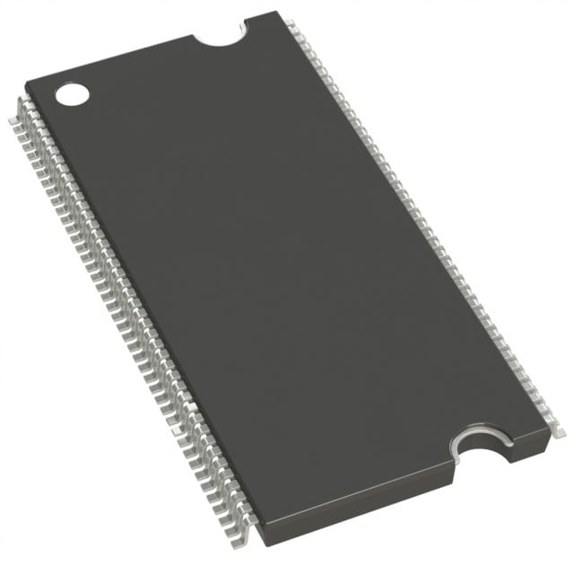
IC DRAM 64MBIT PAR 86TSOP II |
|---|---|
| Quantity | 1,616 Available (as of June 15, 2026) |

| Product Category | Memory |
|---|---|
| Manufacturer | Micron Technology Inc. |
| Manufacturing Status | Obsolete |
| Manufacturer Standard Lead Time | Contact Us |
| Datasheet |
Specifications & Environmental
| Device Package | 86-TSOP II | Memory Format | DRAM | Technology | SDRAM | ||
|---|---|---|---|---|---|---|---|
| Memory Size | 64 Mbit | Access Time | 5.4 ns | Grade | Automotive | ||
| Clock Frequency | 167 MHz | Voltage | 3V ~ 3.6V | Memory Type | Volatile | ||
| Operating Temperature | -40°C ~ 85°C (TA) | Write Cycle Time Word Page | 12 ns | Packaging | 86-TFSOP (0.400", 10.16mm Width) | ||
| Mounting Method | Volatile | Memory Interface | Parallel | Memory Organization | 2M x 32 | ||
| Moisture Sensitivity Level | 3 (168 Hours) | RoHS Compliance | ROHS3 Compliant | REACH Compliance | REACH Unaffected | ||
| Qualification | AEC-Q100 | ECCN | EAR99 | HTS Code | 8542.32.0002 |
Overview of MT48LC2M32B2P-6A AIT:J – IC DRAM 64MBIT PAR 86TSOP II
The MT48LC2M32B2P-6A AIT:J is a 64 Mbit, x32 SDR SDRAM organized as 2M × 32 with internal bank architecture and a parallel memory interface. It is a fully synchronous DRAM device designed for applications requiring pipelined operation, programmable burst lengths and standard SDRAM timing options.
Targeted toward systems that require automotive-grade qualification and extended-temperature operation, this device provides 167 MHz clock operation, a 3.0–3.6 V supply range, and an 86-pin TSOP II (0.400", 10.16 mm width) package for board-level integration.
Key Features
- SDR SDRAM Architecture Fully synchronous SDRAM with all signals registered on the positive edge of the system clock and internal pipelined operation for column switching every clock cycle.
- Memory Organization 2M × 32 organization (512K × 32 × 4 banks) delivering 64 Mbit of storage with internal banks for hiding row access/precharge.
- Performance 167 MHz clock frequency with an access time of 5.4 ns and support for CAS latencies of 1, 2 and 3; programmable burst lengths of 1, 2, 4, 8 or full page.
- Timing Options Cycle-time options include the -6A speed grade (167 MHz / 6 ns cycle time) and related timing parameters documented for RCD, RP and CL.
- Power Single supply operation at 3.0 V to 3.6 V (3.3 V ±0.3 V per datasheet) for standard SDRAM power domains.
- Package 86-pin TSOP II (0.400", 10.16 mm width) plastic package optimized for surface-mount assembly and high-density board layouts.
- Automotive Qualification AEC-Q100 qualification and an operating temperature range of −40 °C to +85 °C (TA) for transport-grade deployments.
- Refresh and Power Modes Auto refresh and self-refresh support (note: self-refresh availability varies by option) with standard 4K refresh cycles and configurable refresh timing.
Typical Applications
- Automotive control modules AEC-Q100 qualification and −40 °C to +85 °C operating range make this SDRAM suitable for embedded storage in vehicle electronics and control units.
- Embedded systems Parallel SDRAM interface and pipelined operation support embedded controllers and processors requiring synchronous burst reads/writes and low-latency access.
- Industrial equipment Extended-temperature operation and robust timing options suit industrial control and instrumentation that need reliable volatile storage.
Unique Advantages
- Automotive-grade qualification: AEC-Q100 qualification provides a documented quality baseline for automotive and transport applications.
- Banked SDRAM architecture: Four internal banks with internal precharge/hide capabilities enable improved throughput for interleaved access patterns.
- Flexible timing and burst control: Programmable burst lengths and support for multiple CAS latencies allow designers to optimize performance for system timing requirements.
- Board-level friendly package: The 86-pin TSOP II (0.400" / 10.16 mm) package provides a compact, surface-mount form factor for dense PCB layouts.
- Standard 3.3 V supply: Operates from 3.0 V to 3.6 V, matching common system power rails for straightforward integration.
Why Choose MT48LC2M32B2P-6A AIT:J?
This Micron 64 Mbit x32 SDRAM balances synchronous SDRAM performance with automotive-grade qualification, making it suitable for designs that demand deterministic timing, programmable burst transfers and robust operation across −40 °C to +85 °C. The 2M × 32 organization with four internal banks supports pipelined and interleaved access patterns common in embedded and control applications.
The 86-pin TSOP II package and standard 3.3 V supply simplify integration into existing boards, while the documented timing options and CAS latency support give designers the flexibility to tune performance to system requirements. The device is appropriate for procurement in designs that require a qualified, parallel SDRAM memory element from a recognized manufacturer.
Request a quote or submit a product inquiry to begin the procurement process for the MT48LC2M32B2P-6A AIT:J.