MT48LC2M32B2P-6A AIT:J TR
| Part Description |
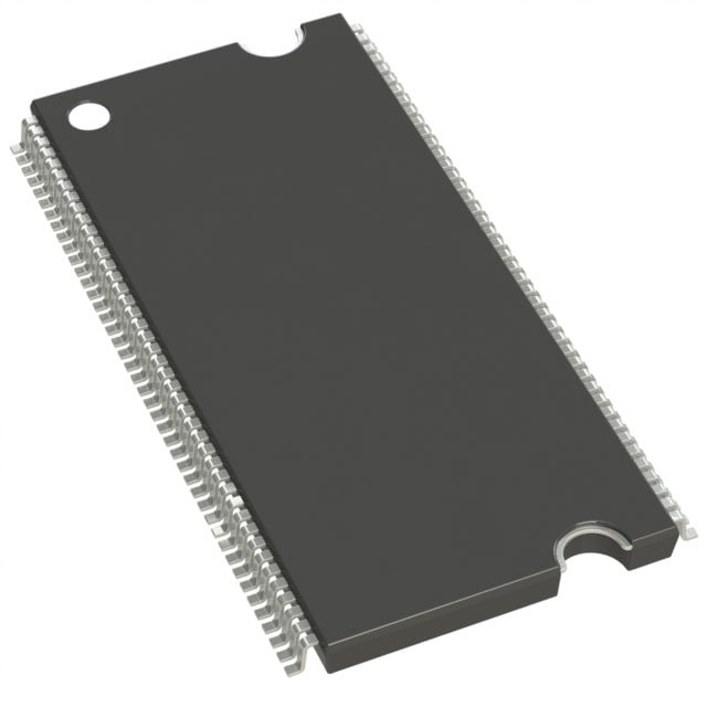
IC DRAM 64MBIT PAR 86TSOP II |
|---|---|
| Quantity | 652 Available (as of June 15, 2026) |

| Product Category | Memory |
|---|---|
| Manufacturer | Micron Technology Inc. |
| Manufacturing Status | Obsolete |
| Manufacturer Standard Lead Time | Contact Us |
| Datasheet |
Specifications & Environmental
| Device Package | 86-TSOP II | Memory Format | DRAM | Technology | SDRAM | ||
|---|---|---|---|---|---|---|---|
| Memory Size | 64 Mbit | Access Time | 5.4 ns | Grade | Automotive | ||
| Clock Frequency | 167 MHz | Voltage | 3V ~ 3.6V | Memory Type | Volatile | ||
| Operating Temperature | -40°C ~ 85°C (TA) | Write Cycle Time Word Page | 12 ns | Packaging | 86-TFSOP (0.400", 10.16mm Width) | ||
| Mounting Method | Volatile | Memory Interface | Parallel | Memory Organization | 2M x 32 | ||
| Moisture Sensitivity Level | 3 (168 Hours) | RoHS Compliance | ROHS3 Compliant | REACH Compliance | REACH Unaffected | ||
| Qualification | AEC-Q100 | ECCN | EAR99 | HTS Code | 8542.32.0002 |
Overview of MT48LC2M32B2P-6A AIT:J TR – IC DRAM 64MBIT PAR 86TSOP II
The MT48LC2M32B2P-6A AIT:J TR is a 64 Mbit SDR SDRAM organized as 2M × 32 with a parallel memory interface. It implements a fully synchronous, pipelined architecture with four internal banks and programmable burst lengths to support system memory buffering and legacy SDRAM applications.
Designed for demanding environments, this device is AEC‑Q100 qualified and specified for operation from −40°C to 85°C (TA), making it suitable for automotive and industrial embedded memory applications that require regulated timing, refresh control, and 3.3 V power rails.
Key Features
- Core / Architecture Fully synchronous SDR SDRAM with internal pipelined operation and four internal banks to enable rapid row/column access and column changes on each clock cycle.
- Memory Organization 2M × 32 configuration delivering 64 Mbit total density with a parallel interface and DRAM memory format.
- Timing & Performance Clock frequency up to 167 MHz (speed grade −6A) with an access time of 5.4 ns and support for CAS latencies (CL) of 1, 2, and 3; programmable burst lengths of 1, 2, 4, 8, or full page.
- Refresh & Power Modes Auto refresh and self refresh modes (self refresh not available on AT devices) with 4096-cycle refresh intervals; single 3.3 V ±0.3 V supply (specified 3.0 V–3.6 V).
- Package & Mounting 86‑pin TSOP II (0.400", 10.16 mm width) package for standard surface‑mount board integration.
- Qualification & Temperature AEC‑Q100 qualification with an operating temperature range of −40°C to 85°C (TA), supporting automotive-grade and industrial applications.
- Compatibility PC100‑compliant signaling with LVTTL‑compatible inputs and outputs for integration into existing SDRAM designs.
Typical Applications
- Automotive Electronics Memory buffer and working RAM in automotive control and infotainment modules where AEC‑Q100 qualification and −40°C to 85°C temperature range are required.
- Industrial Control Embedded SDRAM for industrial controllers and instrumentation requiring synchronous parallel memory and regulated refresh behavior.
- Legacy System Upgrades Replacement or maintenance of PC100‑class SDRAM memory in legacy computing and embedded platforms.
- Buffering and Frame Storage Temporary data storage and burst-oriented buffering in systems that leverage programmable burst lengths and pipelined access.
Unique Advantages
- Automotive-Grade Qualification: AEC‑Q100 qualification and specified −40°C to 85°C operation provide documented reliability for automotive and harsh-environment use.
- Flexible Timing Options: Support for CL = 1, 2, 3 and programmable burst lengths enables tuning for latency or throughput depending on system needs.
- Standard 3.3 V Supply: Operates from 3.0 V to 3.6 V (single 3.3 V ±0.3 V), simplifying power-rail design in systems using legacy SDRAM voltages.
- Compact, Industry-Standard Package: 86‑pin TSOP II (0.400") package offers a compact surface-mount footprint for high‑density board layouts.
- Synchronous, Pipelined Operation: Fully synchronous design with internal banks and pipelining enables column address change every clock cycle for predictable, high-throughput access patterns.
Why Choose MT48LC2M32B2P-6A AIT:J TR?
The MT48LC2M32B2P-6A AIT:J TR combines a proven SDR SDRAM architecture with automotive qualification and a standard TSOP II package to provide a reliable, easy-to-integrate memory option for embedded designs. Its programmable timing, burst control, and pipelined internal banks deliver a balance of latency and throughput suitable for buffering and working memory tasks.
This device is well suited to designers and procurement teams targeting automotive and industrial platforms that require validated parts, predictable SDRAM timing, and a compact 86‑pin footprint for surface-mount assemblies.
If you would like availability, lead time, or a formal quote, request a quote or submit a procurement inquiry to obtain pricing and delivery details for MT48LC2M32B2P-6A AIT:J TR.