MT48LC2M32B2P-6A IT:J
| Part Description |
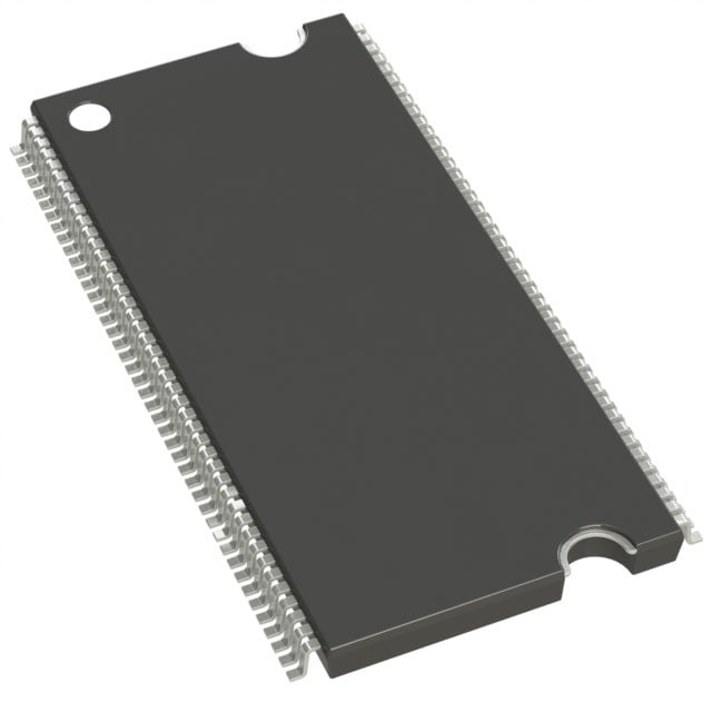
IC DRAM 64MBIT PAR 86TSOP II |
|---|---|
| Quantity | 1,098 Available (as of June 10, 2026) |

| Product Category | Memory |
|---|---|
| Manufacturer | Micron Technology Inc. |
| Manufacturing Status | Obsolete |
| Manufacturer Standard Lead Time | Contact Us |
| Datasheet |
Specifications & Environmental
| Device Package | 86-TSOP II | Memory Format | DRAM | Technology | SDRAM | ||
|---|---|---|---|---|---|---|---|
| Memory Size | 64 Mbit | Access Time | 5.4 ns | Grade | Industrial | ||
| Clock Frequency | 167 MHz | Voltage | 3V ~ 3.6V | Memory Type | Volatile | ||
| Operating Temperature | -40°C ~ 85°C (TA) | Write Cycle Time Word Page | 12 ns | Packaging | 86-TFSOP (0.400", 10.16mm Width) | ||
| Mounting Method | Volatile | Memory Interface | Parallel | Memory Organization | 2M x 32 | ||
| Moisture Sensitivity Level | 3 (168 Hours) | RoHS Compliance | ROHS3 Compliant | REACH Compliance | REACH Unaffected | ||
| Qualification | N/A | ECCN | EAR99 | HTS Code | 8542.32.0002 |
Overview of MT48LC2M32B2P-6A IT:J – IC DRAM 64Mbit, 86-TSOP II
The MT48LC2M32B2P-6A IT:J is a 64 Mbit (2M × 32) synchronous DRAM (SDRAM) device in an 86-pin TSOP II package. It implements a fully synchronous, pipelined architecture with internal bank management and a parallel memory interface for system designs requiring deterministic SDRAM behavior.
Targeted at systems that require a PC100-class SDRAM solution, this part provides a 167 MHz clock rating (–6A speed grade), industrial operating range, and a single 3.0–3.6 V supply window to support reliable operation across a variety of embedded and board-level applications.
Key Features
- Core architecture — 2M × 32 organization with 4 internal banks (512K × 32 × 4 banks) for hidden row access and improved pipeline performance.
- SDR SDRAM functionality — Fully synchronous operation with all signals registered on the positive edge of the system clock; internal pipelined operation allows column address changes every clock cycle.
- Performance — Clock frequency rated at 167 MHz for the –6A grade and an access time of 5.4 ns; supports CAS latencies (CL) of 1, 2, and 3.
- Burst and refresh control — Programmable burst lengths (1, 2, 4, 8, or full page), auto precharge, auto refresh and self-refresh capabilities; 64 ms, 4096-cycle refresh supported per datasheet options.
- Interface and I/O — Parallel memory interface with LVTTL-compatible inputs and outputs for straightforward integration with legacy parallel memory controllers.
- Power — Single-supply operation: 3.0 V to 3.6 V (datasheet: 3.3 V ±0.3 V), supporting standard 3.3 V system rails.
- Timing — Write cycle time (word/page) of 12 ns and documented timing parameters for –6A speed grade (RCD, RP, CL = 18 ns).
- Package — 86-pin TSOP II (0.400", 10.16 mm width) standard footprint (86-TFSOP / 86-TSOP II), suited to compact board layouts.
- Temperature range — Specified operating temperature: –40 °C to +85 °C (TA), supporting industrial-temperature applications.
Typical Applications
- Embedded systems — Provides synchronous parallel DRAM storage for embedded controllers and board-level memory expansion where a 64 Mbit SDRAM is required.
- PC100-class memory designs — Compatible with PC100-class timing and operation for systems designed around PC100 SDRAM parameters.
- Industrial electronics — Industrial temperature rating supports use in systems operating across –40 °C to +85 °C.
Unique Advantages
- Deterministic synchronous operation — Fully synchronous design with pipelined internal operation enables consistent timing behavior for system memory architectures.
- Flexible burst control — Programmable burst lengths and auto precharge/refresh modes simplify system-level memory sequencing and improve effective throughput.
- Industrial temperature range — Specified operation from –40 °C to +85 °C supports deployment in temperature-challenging environments.
- Compact TSOP II package — 86-pin TSOP II (0.400" / 10.16 mm) footprint balances density and serviceability for board-level integration.
- Standard 3.3 V supply compatibility — Operates from 3.0 V to 3.6 V, matching common 3.3 V system rails for ease of power system design.
Why Choose IC DRAM 64MBIT PAR 86TSOP II?
The MT48LC2M32B2P-6A IT:J delivers a documented PC100-class SDRAM implementation in a compact 86-pin TSOP II package with industrial temperature capability and standard 3.3 V supply compatibility. Its 2M × 32 organization, internal bank architecture, and programmable burst/refresh features make it suitable for designs that require a synchronous, parallel DRAM solution with defined timing characteristics.
This part is appropriate for engineers specifying board-level SDRAM where deterministic timing, industrial temperature operation, and a compact TSOP II footprint are required. The combination of speed grade data, timing tables, and power/temperature specifications supports predictable integration and long-term availability in production designs.
Request a quote or submit an inquiry for pricing and availability of the MT48LC2M32B2P-6A IT:J to receive lead-time and ordering information.