
MT48LC2M32B2P-6A IT:J TR
| Part Description |
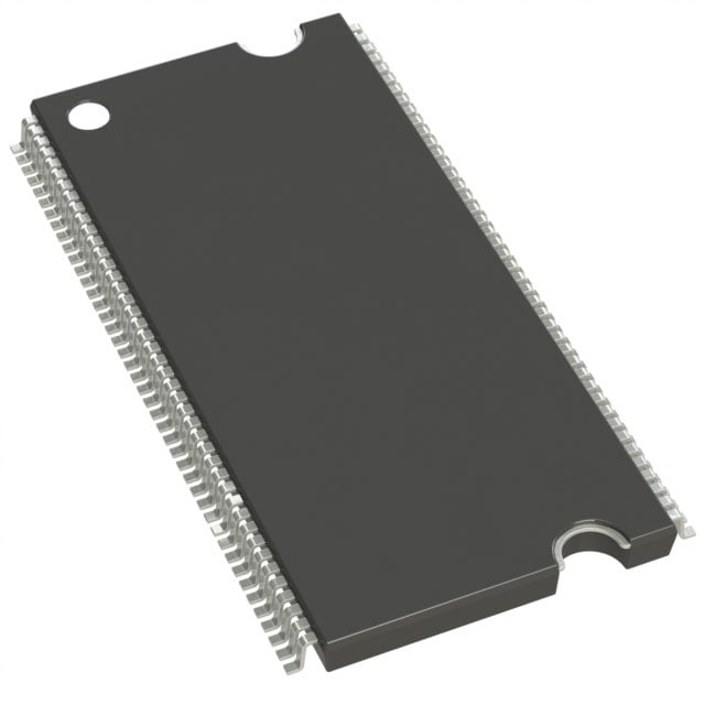
IC DRAM 64MBIT PAR 86TSOP II |
|---|---|
| Quantity | 169 Available (as of June 15, 2026) |
| Product Category | Memory |
|---|---|
| Manufacturer | Micron Technology Inc. |
| Manufacturing Status | Active |
| Manufacturer Standard Lead Time | N/A Weeks |
| Datasheet |
Specifications & Environmental
| Device Package | 86-TSOP II | Memory Format | DRAM | Technology | SDRAM | ||
|---|---|---|---|---|---|---|---|
| Memory Size | 64 Mbit | Access Time | 5.4 ns | Grade | Industrial | ||
| Clock Frequency | 167 MHz | Voltage | 3V ~ 3.6V | Memory Type | Volatile | ||
| Operating Temperature | -40°C ~ 85°C (TA) | Write Cycle Time Word Page | 12 ns | Packaging | 86-TFSOP (0.400", 10.16mm Width) | ||
| Mounting Method | Volatile | Memory Interface | LVTTL | Memory Organization | 2M x 32 | ||
| Moisture Sensitivity Level | N/A | RoHS Compliance | N/A | REACH Compliance | N/A | ||
| Qualification | N/A | ECCN | N/A | HTS Code | N/A |
Overview of MT48LC2M32B2P-6A IT:J TR – IC DRAM 64MBIT PAR 86TSOP II
The MT48LC2M32B2P-6A IT:J TR is a 64 Mbit (2M × 32) synchronous DRAM (SDRAM) device configured as 512K × 32 with 4 internal banks. It implements fully synchronous, pipelined operation with LVTTL-compatible inputs/outputs and is supplied from a single 3.3 V ±0.3 V rail.
Designed for systems requiring PC100‑class SDRAM performance, this device provides programmable burst lengths, internal bank architecture for row‑access hiding, and industrial temperature operation for deployment in extended‑temperature applications.
Key Features
- Core Architecture 2M × 32 organization (512K × 32 × 4 banks) with internal pipelined operation and four internal banks for improved row access efficiency.
- SDRAM Functionality Fully synchronous SDRAM with programmable burst lengths (1, 2, 4, 8, or full page), auto precharge, auto refresh, and self‑refresh mode (self‑refresh not available on AT devices).
- Performance & Timing -6A speed grade with 167 MHz clock frequency; access time listed at 5.4 ns and write cycle time (word page) of 12 ns. Supports CAS latency (CL) values of 1, 2, and 3.
- Refresh Options Auto refresh support with documented 4096‑cycle refresh counts (64 ms / 4096 cycles for commercial and industrial options noted in datasheet).
- Interface & Voltage LVTTL‑compatible inputs/outputs and a single supply of 3.3 V ±0.3 V (3.0 V to 3.6 V operating range).
- Package & Mounting 86‑pin TSOP II (400 mil / 10.16 mm width) package (86‑TFSOP) optimized for compact PCB layouts and standard TSOP II footprint mounting.
- Operating Temperature Industrial temperature range: −40 °C to +85 °C (TA) suitable for extended‑temperature deployments.
- Standards Compliance PC100‑compliant timing and signaling characteristics as specified in the datasheet.
Typical Applications
- PC100‑class memory subsystems — Used where PC100‑compliant SDRAM timing and behavior are required.
- Industrial systems — Industrial temperature range (−40 °C to +85 °C) for extended‑temperature electronics.
- Space‑constrained PCBs — 86‑pin TSOP II (400 mil) package fits compact board layouts requiring a standard TSOP II footprint.
- 3.3 V LVTTL interface designs — Suitable for systems that use LVTTL signaling and a 3.3 V supply rail.
Unique Advantages
- Synchronous pipelined operation: Internal pipelining allows column address changes every clock cycle, enabling predictable, clock‑synchronous data flow.
- Flexible burst control: Programmable burst lengths (1, 2, 4, 8, full page) allow tuning of sequential read/write behavior for system throughput and latency tradeoffs.
- Internal bank architecture: Four internal banks help hide row‑access/precharge overhead and improve effective memory throughput.
- Industrial temperature capability: Rated for −40 °C to +85 °C (TA), supporting deployments in extended‑temperature environments.
- Standardized footprint: Available in a 86‑pin TSOP II (400 mil) package for compatibility with common TSOP II PCB designs.
- PC100 timing class: Documented PC100 compliance and a 167 MHz (‑6A) speed grade provide verified timing behavior for legacy PC100 systems.
Why Choose MT48LC2M32B2P-6A IT:J TR?
The MT48LC2M32B2P-6A IT:J TR offers a compact, industry‑grade 64 Mbit SDRAM solution with synchronous pipelined architecture, programmable burst modes, and LVTTL I/O. Its combination of PC100‑class timing, 167 MHz speed grade, and industrial temperature rating make it well suited to designs that require deterministic SDRAM behavior in constrained board space.
This device is appropriate for engineers specifying a 3.3 V SDRAM with a standard 86‑pin TSOP II package and documented refresh and timing characteristics. The Micron datasheet details timing, refresh, and electrical parameters to support system integration and validation.
Request a quote or submit an inquiry for pricing and availability to review lead times and volume options for the MT48LC2M32B2P-6A IT:J TR.


