MT48LC2M32B2B5-6A:J
| Part Description |
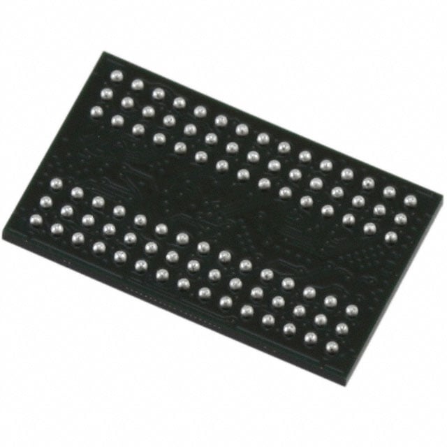
IC DRAM 64MBIT PAR 90VFBGA |
|---|---|
| Quantity | 310 Available (as of June 15, 2026) |

| Product Category | Memory |
|---|---|
| Manufacturer | Micron Technology Inc. |
| Manufacturing Status | Obsolete |
| Manufacturer Standard Lead Time | Contact Us |
| Datasheet |
Specifications & Environmental
| Device Package | 90-VFBGA (8x13) | Memory Format | DRAM | Technology | SDRAM | ||
|---|---|---|---|---|---|---|---|
| Memory Size | 64 Mbit | Access Time | 5.4 ns | Grade | Commercial | ||
| Clock Frequency | 167 MHz | Voltage | 3V ~ 3.6V | Memory Type | Volatile | ||
| Operating Temperature | 0°C ~ 70°C (TA) | Write Cycle Time Word Page | 12 ns | Packaging | 90-VFBGA | ||
| Mounting Method | Volatile | Memory Interface | Parallel | Memory Organization | 2M x 32 | ||
| Moisture Sensitivity Level | 3 (168 Hours) | RoHS Compliance | ROHS3 Compliant | REACH Compliance | REACH Unaffected | ||
| Qualification | N/A | ECCN | EAR99 | HTS Code | 8542.32.0002 |
Overview of MT48LC2M32B2B5-6A:J – IC DRAM 64MBIT PAR 90VFBGA
The MT48LC2M32B2B5-6A:J is a 64 Mbit SDR SDRAM organized as 2M x 32 with a parallel memory interface in a 90-ball VFBGA package. It implements fully synchronous SDRAM architecture with internal pipelining and banked operation to support high-throughput burst access patterns for commercial embedded systems.
Designed for commercial-temperature applications (0°C to +70°C) and single-supply operation around 3.3 V, this device targets systems requiring compact, parallel SDRAM memory with PC100-compliant timing and programmable burst lengths.
Key Features
- Memory Architecture — 64 Mbit SDRAM organized as 2M × 32 with 4 internal banks; supports parallel interface operation and standard DRAM memory format.
- Synchronous SDRAM Operation — Fully synchronous device with all signals registered on the positive edge of the system clock and internal pipelined operation for column-address changes every clock cycle.
- Performance Grades — Speed grade -6A targets a 167 MHz clock frequency; documented timing includes an access time of 5.4 ns and a write cycle time (word page) of 12 ns.
- Programmable Burst and Latency — Programmable burst lengths (1, 2, 4, 8, or full page) and support for CAS latency values of 1, 2, and 3 to match system timing requirements.
- Refresh and Power Management — Supports auto refresh and self refresh modes; 4096-cycle refresh and options for 64 ms/4096-cycle refresh (commercial) as described in the datasheet.
- Voltage and I/O — Single-supply operation at 3.3 V ±0.3 V (listed supply 3.0 V to 3.6 V) with LVTTL-compatible inputs and outputs.
- Compact Package — 90-ball VFBGA (8 mm × 13 mm) package suitable for space-constrained designs.
- Commercial Temperature Range — Rated for operation from 0°C to +70°C (TA).
Typical Applications
- Commercial Embedded Systems — Parallel SDRAM for general-purpose embedded memory in consumer and commercial electronics operating within 0°C to +70°C.
- PC100-Compatible Designs — Systems requiring PC100-compliant SDRAM timing and synchronous operation.
- Buffering and Frame Storage — Burst-capable SDRAM suitable for data buffering and short-term frame or packet storage where parallel memory access is required.
Unique Advantages
- Deterministic Synchronous Operation: All signals registered on the positive edge of the clock and internal pipelining enable predictable timing for system design.
- Flexible Burst Control: Programmable burst lengths and CAS latency support enable tuning of throughput and latency to match application needs.
- High-Density x32 Organization: 2M × 32 organization delivers 64 Mbit in a single compact device, reducing board area for parallel memory implementations.
- Standard Voltage Range: Single 3.3 V supply with tolerance 3.0 V–3.6 V simplifies power sequencing in legacy and contemporary 3.3 V systems.
- Space-Saving VFBGA Package: 90-ball VFBGA (8×13 mm) provides a small footprint for designs with board space constraints.
- Refresh and Low-Power Modes: Auto refresh and self-refresh support help manage data retention and power during idle periods as specified in the datasheet.
Why Choose MT48LC2M32B2B5-6A:J?
The MT48LC2M32B2B5-6A:J combines proven SDR SDRAM architecture with a compact VFBGA package and PC100-compatible timing to meet the needs of commercial embedded designs that require synchronous, parallel memory. Its 2M × 32 organization, programmable burst lengths, and multiple CAS latencies provide designers with flexible options for tuning performance and latency.
This device is suited for designers seeking a verifiable, commercially rated SDRAM solution for buffering, frame storage, and general-purpose embedded memory where a 3.3 V supply and a 0°C to +70°C operating range are acceptable. The documented timing and refresh features give engineers the data needed for reliable system integration and long-term deployment.
Request a quote or contact sales for pricing, lead times, and availability for the MT48LC2M32B2B5-6A:J. Provide your requirements to receive a tailored response on supply and support options.