MT48LC2M32B2TG-6 IT:G
| Part Description |
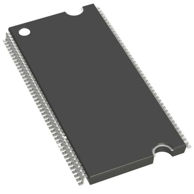
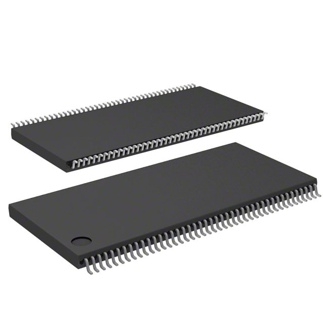
IC DRAM 64MBIT PAR 86TSOP II |
|---|---|
| Quantity | 690 Available (as of June 15, 2026) |

| Product Category | Memory |
|---|---|
| Manufacturer | Micron Technology Inc. |
| Manufacturing Status | Obsolete |
| Manufacturer Standard Lead Time | Contact Us |
| Datasheet |
Specifications & Environmental
| Device Package | 86-TSOP II | Memory Format | DRAM | Technology | SDRAM | ||
|---|---|---|---|---|---|---|---|
| Memory Size | 64 Mbit | Access Time | 5.5 ns | Grade | Industrial | ||
| Clock Frequency | 167 MHz | Voltage | 3V ~ 3.6V | Memory Type | Volatile | ||
| Operating Temperature | -40°C ~ 85°C (TA) | Write Cycle Time Word Page | 12 ns | Packaging | 86-TFSOP (0.400", 10.16mm Width) | ||
| Mounting Method | Volatile | Memory Interface | Parallel | Memory Organization | 2M x 32 | ||
| Moisture Sensitivity Level | 2 (1 Year) | RoHS Compliance | RoHS non-compliant | REACH Compliance | REACH Unaffected | ||
| Qualification | N/A | ECCN | EAR99 | HTS Code | 8542.32.0002 |
Overview of MT48LC2M32B2TG-6 IT:G – IC DRAM 64MBIT PAR 86TSOP II
The MT48LC2M32B2TG-6 IT:G is a 64 Mbit, x32 SDR SDRAM device configured as 2M × 32 (512K × 32 × 4 banks) in an 86-pin TSOP II package. It implements fully synchronous, pipelined SDRAM architecture with a parallel memory interface for systems requiring organized, high-throughput volatile memory.
Designed to operate from a 3.0 V to 3.6 V supply and across an operating ambient range of −40°C to +85°C (TA), the device provides programmable burst control, selectable CAS latencies, and built-in refresh/precharge features for reliable DRAM operation in commercial and industrial applications.
Key Features
- Core / Memory Organization 64 Mbit SDRAM organized as 2M × 32 (512K × 32 × 4 banks) to support banked memory access and internal precharge.
- Synchronous, Pipelined Operation Fully synchronous design with all signals registered on the positive edge of the system clock and internal pipelined operation that allows column address changes every clock cycle.
- Performance & Timing Clock frequency listed at 167 MHz with an access time of 5.5 ns; supports CAS latency (CL) values of 1, 2, and 3 and programmable burst lengths of 1, 2, 4, 8, or full page.
- Refresh & Auto Precharge Auto refresh and auto precharge modes are supported; datasheet specifies 64 ms / 4096-cycle refresh for commercial and industrial options and additional refresh timing options in the product family.
- Interface & Signaling Parallel memory interface with LVTTL-compatible inputs and outputs for standard SDRAM signal levels.
- Power Single 3.3 V ±0.3 V power supply (3.0 V to 3.6 V specified) for device operation.
- Write Cycle Performance Write cycle (word page) timing specified at 12 ns.
- Package & Temperature 86-pin TSOP II (400 mil / 0.400", 10.16 mm width) package; operating ambient temperature range of −40°C to +85°C (TA).
- Standards & Compliance PC100-compliant timing option is listed among the device family’s supported configurations.
Unique Advantages
- Banked SDRAM Architecture: Internal 4-bank organization enables overlapping row access and precharge to improve effective throughput for burst transfers.
- Flexible Burst and Latency Control: Programmable burst lengths and support for multiple CAS latencies let designers match timing to system requirements.
- Industry-Standard Signaling and Supply: LVTTL-compatible I/O and a single 3.3 V ±0.3 V supply simplify interface design with common system logic levels.
- Robust Thermal Range: Specified operation from −40°C to +85°C (TA) supports deployment across commercial and industrial ambient conditions.
- Compact Standard Package: The 86-pin TSOP II form factor (400 mil) provides a space-efficient, supplier-standard package for board-level integration.
Why Choose MT48LC2M32B2TG-6 IT:G?
The MT48LC2M32B2TG-6 IT:G positions itself as a straightforward SDRAM building block for designs that require 64 Mbit of parallel volatile memory with configurable burst behavior and selectable CAS latency. Its fully synchronous, pipelined architecture and LVTTL-compatible interface make it suitable for systems that rely on predictable timing and banked memory access.
This device is suited to designs needing a proven, standardized 86-pin TSOP II package, a 3.0–3.6 V supply domain, and operation across −40°C to +85°C ambient. The combination of programmable timing features and internal refresh/precharge modes provides practical flexibility for integration into established SDRAM-based memory subsystems.
Request a quote or submit an inquiry to obtain pricing, availability and lead-time information for the MT48LC2M32B2TG-6 IT:G.