MT48LC2M32B2P-7:G TR
| Part Description |
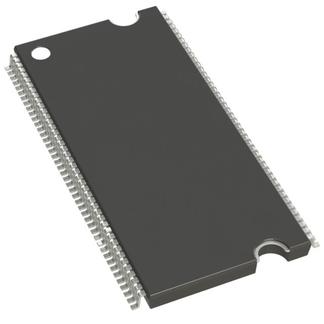
IC DRAM 64MBIT PAR 86TSOP II |
|---|---|
| Quantity | 1,390 Available (as of June 15, 2026) |

| Product Category | DRAM Memory |
|---|---|
| Manufacturer | Micron Technology Inc. |
| Manufacturing Status | Obsolete |
| Manufacturer Standard Lead Time | Contact Us |
| Datasheet |
Specifications & Environmental
| Device Package | 86-TSOP II | Memory Format | DRAM | Technology | SDRAM | ||
|---|---|---|---|---|---|---|---|
| Memory Size | 64 Mbit | Access Time | 5.5 ns | Grade | Commercial | ||
| Clock Frequency | 143 MHz | Voltage | 3V ~ 3.6V | Memory Type | Volatile | ||
| Operating Temperature | 0°C ~ 70°C (TA) | Write Cycle Time Word Page | 14 ns | Packaging | 86-TFSOP (0.400", 10.16mm Width) | ||
| Mounting Method | Volatile | Memory Interface | Parallel | Memory Organization | 2M x 32 | ||
| Moisture Sensitivity Level | 2 (1 Year) | RoHS Compliance | ROHS Compliant | REACH Compliance | REACH Unaffected | ||
| Qualification | N/A | ECCN | EAR99 | HTS Code | 8542.32.0002 |
Overview of MT48LC2M32B2P-7:G TR – IC DRAM 64MBIT PAR 86TSOP II
The MT48LC2M32B2P-7:G TR is a 64 Mbit (2M × 32) SDR SDRAM device in an 86-pin TSOP II (400 mil) package designed for parallel memory interfaces. It implements fully synchronous operation with internal pipelining and multiple banks to support high-throughput read/write cycles for board-level memory subsystems.
Targeted at systems that require a standard 64Mb ×32 SDRAM footprint, the device delivers PC100-compliant operation at a 143 MHz clock frequency with documented timing parameters and power requirements for reliable integration.
Key Features
- Core Architecture Fully synchronous SDR SDRAM with internal pipelined operation and 4 internal banks to hide row access and precharge latency.
- Memory Organization 2M × 32 organization (512K × 32 × 4 banks) providing 64 Mbit capacity in a single-device solution.
- Performance & Timing PC100-compliant; specified for a 143 MHz clock frequency (speed grade -7) with an access time of 5.5 ns and a write cycle time (word/page) of 14 ns. Supports CAS latency (CL) settings of 1, 2 and 3.
- Burst & Command Flexibility Programmable burst lengths (1, 2, 4, 8 or full page), auto precharge and auto refresh modes, plus self-refresh capability (note: self-refresh not available on AT devices as specified).
- Power Single-supply operation at 3.3 V nominal with an allowed range of 3.0 V to 3.6 V.
- Interface & I/O Parallel memory interface with LVTTL-compatible inputs and outputs for standard system-level interoperability.
- Packaging 86-TFSOP / 86-pin TSOP II (0.400", 10.16 mm width) footprint for board-level installations; available in standard and Pb-free package options as listed in device options.
- Operating Range Commercial temperature range specified at 0°C to +70°C (TA).
- Refresh Supports auto refresh with documented refresh schemes (e.g., 64 ms / 4096-cycle for commercial timing) and industry-standard refresh counts.
Typical Applications
- System Memory Subsystems Used as board-level SDRAM for processors and controllers that require a parallel SDRAM interface with 64 Mbit ×32 capacity.
- Legacy and Embedded Designs Fits designs that utilize an 86-pin TSOP II footprint and need PC100-compliant synchronous DRAM timing.
- Buffered Read/Write Buffers Suitable for applications requiring internal bank-based hiding of row access/precharge to support pipelined read/write operations.
Unique Advantages
- Standard PC100 Compatibility: Ensures predictable timing and interoperability in systems designed to PC100 SDRAM specifications.
- Flexible Burst Modes: Programmable burst lengths (1, 2, 4, 8, full page) allow tuning data transfer patterns to match system access needs.
- Low-Voltage 3.3 V Operation: Single 3.3 V supply simplifies power rail design while meeting the specified 3.0 V–3.6 V range.
- Compact TSOP II Footprint: 86-pin TSOP II package provides a compact, board-friendly form factor for designs constrained by PCB area.
- Documented Timing and Refresh: Datasheet includes explicit timing tables, CAS latency options, and refresh schemes to support deterministic memory design and validation.
Why Choose MT48LC2M32B2P-7:G TR?
The MT48LC2M32B2P-7:G TR positions itself as a well-documented, standard-form-factor SDRAM device for designs requiring 64 Mbit ×32 parallel memory in an 86-pin TSOP II package. With PC100 compliance, programmable burst operation, and multiple CAS latency options, it provides designers with the timing flexibility and predictable behavior needed for synchronous memory subsystems.
This device is suited to engineers and procurement teams implementing board-level DRAM capacity where a compact TSOP II package, 3.3 V supply compatibility, and commercial temperature operation (0°C to +70°C) align with system requirements. Comprehensive datasheet timing and refresh information supports integration, validation, and long-term maintenance of deployed designs.
Request a quote or submit a procurement inquiry to begin pricing and availability verification for the MT48LC2M32B2P-7:G TR.