
MT48LC2M32B2P-7:G
| Part Description |
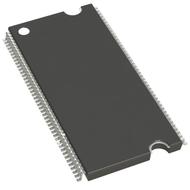
IC DRAM 64MBIT PAR 86TSOP II |
|---|---|
| Quantity | 1,022 Available (as of June 18, 2026) |
| Product Category | DRAM Memory |
|---|---|
| Manufacturer | Micron Technology Inc. |
| Manufacturing Status | Obsolete |
| Manufacturer Standard Lead Time | Contact Us |
| Datasheet |
Specifications & Environmental
| Device Package | 86-TSOP II | Memory Format | DRAM | Technology | SDRAM | ||
|---|---|---|---|---|---|---|---|
| Memory Size | 64 Mbit | Access Time | 5.5 ns | Grade | Commercial | ||
| Clock Frequency | 143 MHz | Voltage | 3V ~ 3.6V | Memory Type | Volatile | ||
| Operating Temperature | 0°C ~ 70°C (TA) | Write Cycle Time Word Page | 14 ns | Packaging | 86-TFSOP (0.400", 10.16mm Width) | ||
| Mounting Method | Volatile | Memory Interface | Parallel | Memory Organization | 2M x 32 | ||
| Moisture Sensitivity Level | 3 (168 Hours) | RoHS Compliance | ROHS Compliant | REACH Compliance | REACH Unaffected | ||
| Qualification | N/A | ECCN | EAR99 | HTS Code | 8542.32.0002 |
Overview of MT48LC2M32B2P-7:G – IC DRAM 64MBIT PAR 86TSOP II
The MT48LC2M32B2P-7:G is a 64 Mbit, 2M × 32 SDRAM organized as 512K × 32 × 4 banks in an 86-pin TSOP II package. It is a fully synchronous SDR SDRAM device designed for parallel memory interfaces and board-level system memory implementations.
Designed with programmable burst lengths, internal pipelining and bank architecture, this device targets PC100‑compliant memory designs and parallel SDRAM applications that require a compact TSOP II form factor, single 3.3 V power supply operation, and commercial temperature operation.
Key Features
- Core architecture Fully synchronous SDR SDRAM with all signals registered on the positive edge of the system clock and internal pipelined operation for column address changes each clock cycle.
- Memory organization 2M × 32 configuration (512K × 32 × 4 banks) delivering a total of 64 Mbit in a x32 data width.
- Programmable bursts & bank management Supports programmable burst lengths (1, 2, 4, 8, or full page) and internal banks to hide row access and precharge latencies.
- Performance and timing Speed grade -7 with a target clock frequency of 143 MHz; supports CAS latencies (CL) of 1, 2, and 3. Listed access time is 5.5 ns and write cycle time (word page) is 14 ns.
- Power Single 3.3 V supply operation (3.0 V to 3.6 V range) compatible with LVTTL I/O signaling.
- Refresh and reliability features Auto refresh and self‑refresh modes supported; 4K refresh count options with 64 ms/4096‑cycle refresh noted for commercial/industrial ranges in the datasheet.
- Package 86‑pin TSOP II (0.400", 10.16 mm width) standard package, supplied as 86‑TSOP II.
- Operating range Commercial temperature range: 0°C to +70°C (TA).
Typical Applications
- PC100-compliant memory subsystems Use where PC100 timing compatibility and standard SDRAM interfaces are required.
- Board-level parallel memory Embedded boards and legacy systems that require a parallel SDRAM x32 device in a compact TSOP II package.
- System memory with burst access Designs that benefit from programmable burst lengths and internal bank architecture to improve sustained throughput for sequential accesses.
Unique Advantages
- Compact TSOP II footprint: Provides 64 Mbit of x32 SDRAM in an 86‑pin, 400 mil package (10.16 mm width) for space‑constrained board designs.
- Synchronous pipelined operation: Registered inputs on the positive clock edge and internal pipelining allow column addresses to change each clock cycle, simplifying timing for synchronous memory systems.
- Flexible burst control: Programmable burst lengths (including full‑page) let designers tune transfer granularity for a range of access patterns.
- Standard voltage and I/O compatibility: Single 3.3 V supply range (3.0–3.6 V) and LVTTL‑compatible I/O simplify integration with legacy 3.3 V logic domains.
- Robust refresh support: Auto refresh and self‑refresh modes with documented refresh counts reduce system refresh management overhead.
Why Choose MT48LC2M32B2P-7:G?
The MT48LC2M32B2P-7:G combines a compact 86‑pin TSOP II package with a standard, fully synchronous SDRAM architecture (2M × 32, 4 banks), making it suitable for designs that require parallel SDRAM in constrained form factors. Its PC100‑level timing compatibility, programmable burst lengths and LVTTL I/O support facilitate integration into existing board‑level memory subsystems.
This device is well suited to engineers specifying commercial‑temperature, 3.3 V SDRAM for systems that need predictable synchronous timing, flexible burst modes and standard refresh features. The documented timing grades and package details support straightforward BOM and layout planning for refurbishment, repair, or new designs that rely on x32 SDRAM components.
For pricing, availability, or to request a quote for the MT48LC2M32B2P-7:G, submit a sales inquiry to discuss lead times and ordering options.


