MT48LC2M32B2TG-55:G TR
| Part Description |
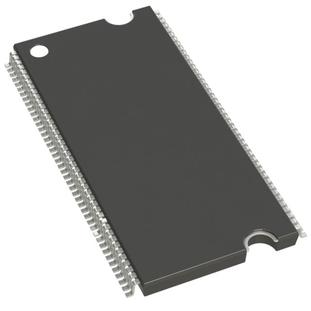
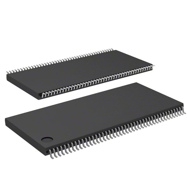
IC DRAM 64MBIT PAR 86TSOP II |
|---|---|
| Quantity | 349 Available (as of June 13, 2026) |

| Product Category | Memory |
|---|---|
| Manufacturer | Micron Technology Inc. |
| Manufacturing Status | Obsolete |
| Manufacturer Standard Lead Time | Contact Us |
| Datasheet |
Specifications & Environmental
| Device Package | 86-TSOP II | Memory Format | DRAM | Technology | SDRAM | ||
|---|---|---|---|---|---|---|---|
| Memory Size | 64 Mbit | Access Time | 5 ns | Grade | Commercial | ||
| Clock Frequency | 183 MHz | Voltage | 3V ~ 3.6V | Memory Type | Volatile | ||
| Operating Temperature | 0°C ~ 70°C (TA) | Write Cycle Time Word Page | N/A | Packaging | 86-TFSOP (0.400", 10.16mm Width) | ||
| Mounting Method | Volatile | Memory Interface | Parallel | Memory Organization | 2M x 32 | ||
| Moisture Sensitivity Level | 2 (1 Year) | RoHS Compliance | RoHS non-compliant | REACH Compliance | REACH Unaffected | ||
| Qualification | N/A | ECCN | EAR99 | HTS Code | 8542.32.0002 |
Overview of MT48LC2M32B2TG-55:G TR – IC DRAM 64MBIT PAR 86TSOP II
The MT48LC2M32B2TG-55:G TR is a 64 Mbit SDR SDRAM organized as 2M × 32 with a parallel memory interface in an 86‑pin TSOP II package. It implements a fully synchronous, pipelined architecture with four internal banks and programmable burst lengths to support predictable, cycle-aligned memory transfers.
Designed for systems that require a 64 Mbit ×32 SDRAM footprint, the device delivers operation at a clock frequency of 183 MHz, supports CAS latencies of 1, 2 and 3, and operates from a single 3.0 V–3.6 V supply across a 0 °C to +70 °C ambient range.
Key Features
- Core architecture Fully synchronous SDR SDRAM with all signals registered on the positive edge of the system clock and internal pipelined operation allowing column address changes every clock cycle.
- Memory organization 64 Mbit capacity organized as 2M × 32 with four internal banks (512K × 32 × 4 banks).
- Performance & timing Target clock frequency 183 MHz (speed grade -55) with support for CAS latency (CL) = 1, 2, 3; timing target for -55 is 3-3-3 with 16.5 ns RCD/RP/CL.
- Programmable burst lengths Selectable burst lengths of 1, 2, 4, 8 or full page to match access patterns and bus efficiency requirements.
- Refresh and power modes Auto refresh and self-refresh modes supported; 4096-cycle refresh with 64 ms (commercial) timing as specified.
- Interface & I/O Parallel memory interface with LVTTL-compatible inputs and outputs for standard logic-level integration.
- Supply & power Single supply operation at 3.3 V ±0.3 V (listed supply range 3.0 V–3.6 V).
- Package & temperature 86‑pin TSOP II (400 mil / 10.16 mm width) standard package; commercial operating range 0 °C to +70 °C (TA).
Typical Applications
- Board-level SDRAM memory Provides 64 Mbit ×32 parallel SDRAM in an 86‑pin TSOP II footprint for systems requiring synchronous DRAM.
- Legacy SDR system upgrades Drop-in compatible memory for designs specifying 2M × 32 SDR SDRAM with standard timing and supply requirements.
- Embedded system buffers Use as a shared data buffer where programmable burst lengths and pipelined bank operation improve throughput.
Unique Advantages
- Predictable synchronous operation: Positive-edge clocked, fully synchronous design ensures consistent timing behavior across system clocks.
- Flexible access patterns: Programmable burst lengths and internal bank architecture allow efficient handling of both short and burst transfers.
- Standard voltage compatibility: Single 3.3 V supply range (3.0 V–3.6 V) simplifies power rail design in existing 3.3 V systems.
- Compact package: 86‑pin TSOP II package provides a high-density memory option in a standardized footprint.
- Defined timing grade: -55 speed grade with 183 MHz clock targeting 3-3-3 timing (16.5 ns RCD/RP/CL) for known performance characteristics.
Why Choose MT48LC2M32B2TG-55:G TR?
The MT48LC2M32B2TG-55:G TR pairs a 64 Mbit ×32 SDRAM organization with a fully synchronous, pipelined architecture and selectable burst modes to deliver predictable, board-level memory performance. Its -55 timing grade and LVTTL-compatible I/O simplify integration into systems designed around a 3.3 V supply and 86‑pin TSOP II form factor.
This device is well suited to designs that require standardized SDR SDRAM behavior, clear timing targets, and commercial temperature operation. It offers a balanced combination of performance, package density, and interface compatibility for engineers specifying parallel SDRAM memory in established 3.3 V systems.
Request a quote or submit a sales inquiry to receive pricing, availability and ordering information for MT48LC2M32B2TG-55:G TR.