MT48LC2M32B2TG-5:G
| Part Description |
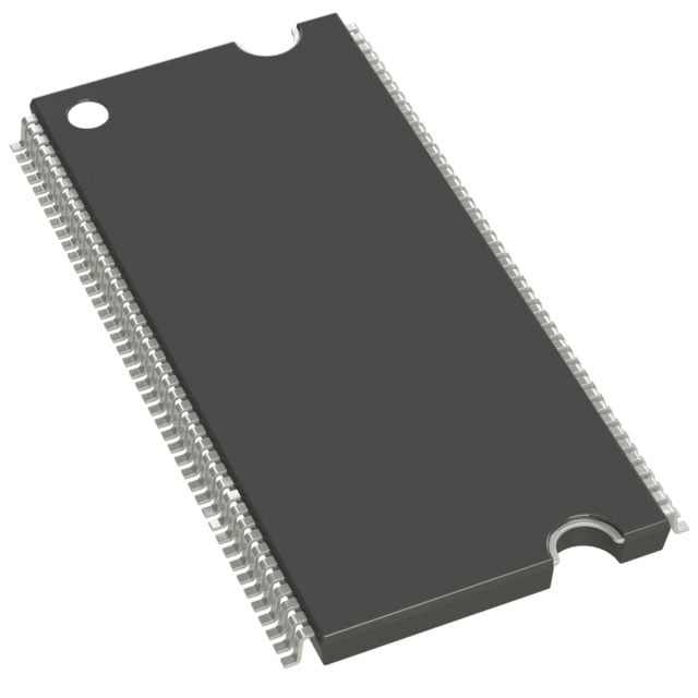
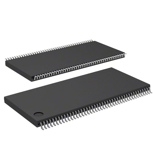
IC DRAM 64MBIT PAR 86TSOP II |
|---|---|
| Quantity | 691 Available (as of June 15, 2026) |

| Product Category | DRAM Memory |
|---|---|
| Manufacturer | Micron Technology Inc. |
| Manufacturing Status | Obsolete |
| Manufacturer Standard Lead Time | Contact Us |
| Datasheet |
Specifications & Environmental
| Device Package | 86-TSOP II | Memory Format | DRAM | Technology | SDRAM | ||
|---|---|---|---|---|---|---|---|
| Memory Size | 64 Mbit | Access Time | 4.5 ns | Grade | Commercial | ||
| Clock Frequency | 200 MHz | Voltage | 3V ~ 3.6V | Memory Type | Volatile | ||
| Operating Temperature | 0°C ~ 70°C (TA) | Write Cycle Time Word Page | N/A | Packaging | 86-TFSOP (0.400", 10.16mm Width) | ||
| Mounting Method | Volatile | Memory Interface | Parallel | Memory Organization | 2M x 32 | ||
| Moisture Sensitivity Level | 2 (1 Year) | RoHS Compliance | RoHS non-compliant | REACH Compliance | REACH Unaffected | ||
| Qualification | N/A | ECCN | EAR99 | HTS Code | 8542.32.0002 |
Overview of MT48LC2M32B2TG-5:G – IC DRAM 64MBIT PAR 86TSOP II
The MT48LC2M32B2TG-5:G is a 64 Mbit synchronous DRAM (SDR SDRAM) organized as 2M × 32 with a parallel memory interface in an 86‑pin TSOP II package. It implements a fully synchronous architecture with internal pipelined operation and multiple internal banks to improve data throughput for systems using PC100-class SDRAM.
Designed for commercial temperature operation, this device targets embedded and system memory applications that require a compact TSOP II footprint, a single 3.3 V supply range, and configurable burst and latency options to match system timing requirements.
Key Features
- Core Architecture Fully synchronous SDR SDRAM with all signals registered on the positive edge of the system clock and internal pipelined operation for column-address changes every clock cycle.
- Memory Organization 64 Mbit capacity organized as 2M × 32 (512K × 32 × 4 banks), providing four internal banks to hide row access and precharge operations.
- Performance / Timing 5 ns (200 MHz) speed grade (-5) with listed access time of 4.5 ns and support for CAS latencies (CL) of 1, 2, and 3.
- Burst and Command Flexibility Programmable burst lengths (1, 2, 4, 8, or full page), auto precharge, auto refresh, and self‑refresh capability (self‑refresh not available on AT devices as noted in product documentation).
- Power and I/O Single 3.3 V power supply (3.3 V ±0.3 V; spec range 3.0 V–3.6 V) with LVTTL‑compatible inputs and outputs.
- Refresh Auto refresh support with commercial refresh timing of 64 ms / 4096 cycles as specified for the device.
- Package and Temperature 86‑pin TSOP II (0.400", 10.16 mm width) package; commercial operating temperature range 0°C to +70°C.
- Interface Parallel memory interface suitable for systems designed around PC100-class SDRAM timing and signaling.
Typical Applications
- PC100-class systems Memory subsystem implementations where PC100‑compliant SDRAM timing and a 200 MHz speed grade are required.
- Embedded system memory System DRAM for embedded designs that need a 64 Mbit parallel SDRAM in a compact 86‑pin TSOP II package.
- Commercial electronics Consumer and commercial devices operating within 0°C to +70°C that require synchronous DRAM with programmable burst and latency options.
- Board-level memory expansion Add-on or replacement memory in designs using standard parallel SDRAM interfaces and LVTTL signaling.
Unique Advantages
- PC100-compliant 200 MHz speed grade Provides a defined 5 ns cycle time (-5) for designs targeting PC100-class timing.
- Flexible timing and bursts Programmable burst lengths and support for CL = 1, 2, 3 let system designers match memory behavior to system timing and throughput needs.
- Banked architecture for throughput Four internal banks and pipelined operation help hide row access and precharge latency, improving effective data transfer rates.
- Standard 3.3 V supply and LVTTL I/O Simplifies interface design with a single supply range (3.0 V–3.6 V) and LVTTL‑compatible signaling.
- Compact TSOP II package 86‑pin TSOP II (400 mil) footprint for space‑constrained board designs while retaining a parallel interface.
- Commercial temperature rating Specified for 0°C to +70°C operation for use in a wide range of commercial applications.
Why Choose MT48LC2M32B2TG-5:G?
The MT48LC2M32B2TG-5:G combines a compact 86‑pin TSOP II package with a fully synchronous SDRAM architecture and a 200 MHz speed grade to serve PC100-class and embedded memory requirements. Its programmable burst lengths, CAS latency options, and four internal banks provide designers with the flexibility to tune performance for specific system timing and throughput needs.
This device is suited for commercial systems that require a 64 Mbit parallel SDRAM with a standard 3.3 V supply, LVTTL I/O compatibility, and defined refresh and timing characteristics. It offers a clear specification set for procurement and integration into board-level memory subsystems.
Request a quote or submit an inquiry to our sales team for pricing, availability, and lead-time information for MT48LC2M32B2TG-5:G.