MT48LC32M16A2P-75:C
| Part Description |
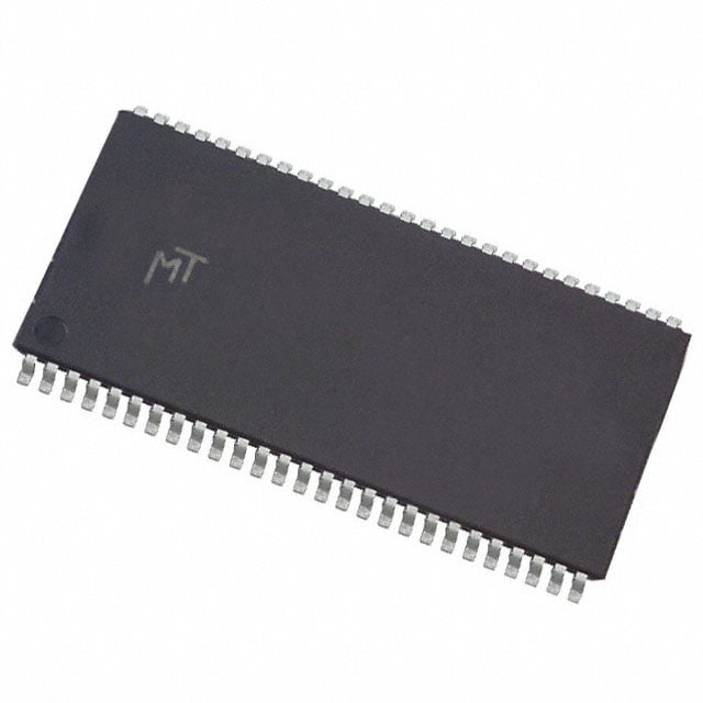
IC DRAM 512MBIT PAR 54TSOP II |
|---|---|
| Quantity | 378 Available (as of June 16, 2026) |

| Product Category | DRAM Memory |
|---|---|
| Manufacturer | Micron Technology Inc. |
| Manufacturing Status | Obsolete |
| Manufacturer Standard Lead Time | Contact Us |
| Datasheet |
Specifications & Environmental
| Device Package | 54-TSOP II | Memory Format | DRAM | Technology | SDRAM | ||
|---|---|---|---|---|---|---|---|
| Memory Size | 512 Mbit | Access Time | 5.4 ns | Grade | Commercial | ||
| Clock Frequency | 133 MHz | Voltage | 3V ~ 3.6V | Memory Type | Volatile | ||
| Operating Temperature | 0°C ~ 70°C (TA) | Write Cycle Time Word Page | 15 ns | Packaging | 54-TSOP (0.400", 10.16mm Width) | ||
| Mounting Method | Volatile | Memory Interface | Parallel | Memory Organization | 32M x 16 | ||
| Moisture Sensitivity Level | N/A | RoHS Compliance | N/A | REACH Compliance | N/A | ||
| Qualification | N/A | ECCN | N/A | HTS Code | N/A |
Overview of MT48LC32M16A2P-75:C – IC DRAM 512MBIT PAR 54TSOP II
The MT48LC32M16A2P-75:C is a 512Mbit synchronous DRAM device organized as 32M × 16 with a parallel memory interface. It implements fully synchronous SDRAM architecture with internal pipelined operation, internal banks and programmable burst lengths for system memory functions that target PC100/PC133-class synchronous designs.
Key electrical and mechanical characteristics include a 133 MHz clock rating (speed grade -75), 3.0 V to 3.6 V supply range, 54-pin TSOP II packaging, and a commercial operating temperature range of 0 °C to 70 °C.
Key Features
- SDR SDRAM architecture – Fully synchronous operation with all signals registered on the positive clock edge and internal pipelining for column-address changes every clock cycle.
- Memory organization – 512 Mbit capacity organized as 32M × 16 with 4 internal banks (8M × 16 × 4 banks configuration).
- PC100/PC133 compliance – Specified as PC100- and PC133-compliant with a 133 MHz clock frequency for the -75 speed grade.
- Low latency and timing – Access time down to 5.4 ns (CL = 3 at 133 MHz) and write cycle time (word/page) of 15 ns as specified.
- Programmable burst and refresh – Programmable burst lengths (1, 2, 4, 8, or full page), auto precharge, auto refresh and self-refresh support with 64 ms / 8192-cycle refresh.
- LVTTL-compatible I/O and single-supply operation – LVTTL inputs/outputs and single 3.3 V ±0.3 V supply (3.0 V–3.6 V) for system-level integration.
- Package and mounting – 54-pin TSOP II (400 mil / 10.16 mm width) surface-mount package for compact board-level deployment.
- Commercial temperature rating – Specified operating range of 0 °C to +70 °C (TA) for commercial applications.
Typical Applications
- PC100/PC133-class memory subsystems – Provides synchronous DRAM capacity and timing compatible with PC100/PC133 system designs.
- System memory expansion – Used where 512 Mbit parallel SDRAM organized as 32M × 16 is required on a 3.3 V supply.
- Commercial embedded systems – Suitable for commercial-temperature embedded designs that require synchronous DRAM with self-refresh and auto-refresh capabilities.
Unique Advantages
- Verified PC100/PC133 timing – Specified compliance with PC100 and PC133 timing simplifies integration into designs targeting those clock classes.
- Flexible burst operation – Programmable burst lengths and internal pipelining enable efficient data transfers and simplified controller timing.
- Integrated refresh modes – Auto refresh and self-refresh plus 8K refresh cycle support reduce external refresh management overhead.
- Compact surface-mount package – 54-pin TSOP II package provides a small footprint for higher-density board layouts.
- Standard 3.3 V supply – Operates from a single 3.0 V–3.6 V supply, aligning with common system voltage rails.
Why Choose IC DRAM 512MBIT PAR 54TSOP II?
The MT48LC32M16A2P-75:C delivers a compact, commercially rated 512 Mbit SDRAM solution with PC100/PC133-compliant timing, internal banking, and programmable burst modes to support synchronous system memory needs. Its 54-pin TSOP II package and 3.3 V single-supply operation make it suitable for designs that require standard parallel SDRAM capacity and predictable timing.
This device is well suited for engineers and procurement teams specifying memory for commercial systems that require reliable synchronous DRAM behavior, refresh management, and compact board-level integration. Its documented timing parameters and package details support straightforward evaluation and long-term design planning.
Request a quote or submit a specification inquiry to receive pricing and availability for the MT48LC32M16A2P-75:C.