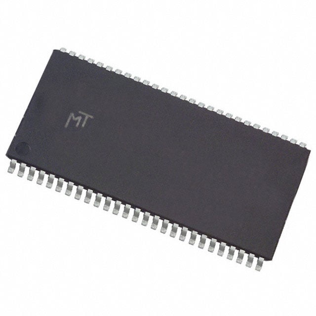
MT48LC32M8A2P-6A IT:G
| Part Description |
IC DRAM 256MBIT PAR 54TSOP II |
|---|---|
| Quantity | 524 Available (as of June 15, 2026) |

| Product Category | Memory |
|---|---|
| Manufacturer | Micron Technology Inc. |
| Manufacturing Status | Obsolete |
| Manufacturer Standard Lead Time | Contact Us |
| Datasheet |
Specifications & Environmental
| Device Package | 54-TSOP II | Memory Format | DRAM | Technology | SDRAM | ||
|---|---|---|---|---|---|---|---|
| Memory Size | 256 Mbit | Access Time | 5.4 ns | Grade | Industrial | ||
| Clock Frequency | 167 MHz | Voltage | 3V ~ 3.6V | Memory Type | Volatile | ||
| Operating Temperature | -40°C ~ 85°C (TA) | Write Cycle Time Word Page | 12 ns | Packaging | 54-TSOP (0.400", 10.16mm Width) | ||
| Mounting Method | Volatile | Memory Interface | Parallel | Memory Organization | 32M x 8 | ||
| Moisture Sensitivity Level | 3 (168 Hours) | RoHS Compliance | ROHS3 Compliant | REACH Compliance | REACH Unaffected | ||
| Qualification | N/A | ECCN | EAR99 | HTS Code | 8542.32.0024 |
Overview of MT48LC32M8A2P-6A IT:G – IC DRAM 256Mbit PAR 54TSOP II
The MT48LC32M8A2P-6A IT:G is a 256 Mbit synchronous DRAM device organized as 32M × 8 with a parallel memory interface in a 54-pin TSOP II package. It implements fully synchronous SDRAM architecture with internal pipelined operation and multiple internal banks.
Targeted at systems requiring PC100/PC133-class SDRAM timing and industrial temperature operation, the device delivers high-speed operation up to 167 MHz while operating from a single 3.3 V ±0.3 V supply (3.0–3.6 V) and an industrial ambient temperature range of −40 °C to +85 °C.
Key Features
- Core / Architecture Fully synchronous SDRAM with internal pipelined operation and multiple internal banks for hidden row access and precharge.
- Memory Organization 256 Mbit density organized as 32M × 8 with four internal banks.
- Performance / Timing Speed grade -6A supports 167 MHz system clock with typical CL = 3 timing; access time listed as 5.4 ns and write cycle time (word/page) of 12 ns.
- Burst and Refresh Programmable burst lengths (1, 2, 4, 8, or full page), auto precharge, auto refresh and self-refresh modes; 8192-cycle refresh supported.
- Voltage and I/O Single 3.3 V ±0.3 V power supply with LVTTL-compatible inputs and outputs; operating supply range 3.0–3.6 V.
- Package & Mounting 54-pin TSOP II (0.400", 10.16 mm width) plastic package intended for board-level mounting.
- Industrial Temperature Range Rated for −40 °C to +85 °C ambient (TA) for industrial applications.
Typical Applications
- PC and Legacy System Memory Designed for systems requiring PC100/PC133-compliant SDRAM timing and synchronous operation.
- Industrial Embedded Systems Industrial temperature rating (−40 °C to +85 °C) and standard 3.3 V supply make it suitable for industrial controllers and embedded platforms.
- Board-Level Data Buffering Parallel interface and programmable burst lengths support buffering and burst transfer use cases in board-level memory subsystems.
- High-Speed Memory Arrays 32M × 8 organization and internal banks enable use in designs requiring moderate density synchronous DRAM.
Unique Advantages
- High clock-rate capability: Supports a 167 MHz clock (speed grade -6A), enabling low-latency synchronous memory operation when used with matching system timing.
- Flexible burst control: Programmable burst lengths (1, 2, 4, 8, full page) allow designers to optimize transfer granularity for throughput or latency.
- Industrial temperature support: Specified for −40 °C to +85 °C ambient operation to meet industrial application thermal requirements.
- Standard 3.3 V supply: Operates from a single 3.3 V ±0.3 V supply (3.0–3.6 V), simplifying power design in existing 3.3 V systems.
- Compact TSOP II footprint: 54-pin TSOP II package (0.400", 10.16 mm width) provides a compact, board-level mount option for space-constrained designs.
- Synchronous, pipelined operation: All signals registered on the positive clock edge with internal pipelining and multiple banks to improve effective throughput in burst transfers.
Why Choose MT48LC32M8A2P-6A IT:G?
The MT48LC32M8A2P-6A IT:G is a straightforward, industry-temperature SDRAM offering 256 Mbit density with synchronous, pipelined operation and PC100/PC133-class timing. Its combination of 32M × 8 organization, programmable burst lengths, and a 54-pin TSOP II package makes it appropriate for embedded and industrial designs that require standard 3.3 V operation and a compact board-level memory solution.
This device is suited to engineers specifying reliable, synchronous DRAM for systems where established SDRAM feature sets (auto refresh, self-refresh, internal banks) and industrial temperature range are required. Its clear electrical and timing characteristics simplify integration into designs that match PC100/PC133 timing or that need a 167 MHz capable memory element.
If you need pricing, availability or a formal quote for MT48LC32M8A2P-6A IT:G, request a quote or submit an inquiry for sales and ordering information.