MT48LC32M8A2BB-7E:G TR
| Part Description |
IC DRAM 256MBIT PARALLEL 60FBGA |
|---|---|
| Quantity | 1,097 Available (as of June 18, 2026) |

| Product Category | DRAM Memory |
|---|---|
| Manufacturer | Micron Technology Inc. |
| Manufacturing Status | Obsolete |
| Manufacturer Standard Lead Time | Contact Us |
| Datasheet |
Specifications & Environmental
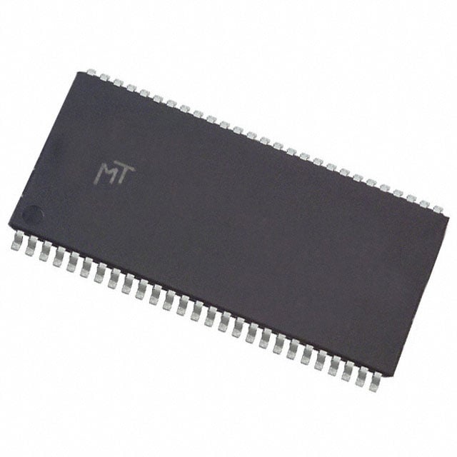
| Device Package | 60-FBGA (8x16) | Memory Format | DRAM | Technology | SDRAM | ||
|---|---|---|---|---|---|---|---|
| Memory Size | 256 Mbit | Access Time | 5.4 ns | Grade | Commercial | ||
| Clock Frequency | 133 MHz | Voltage | 3V ~ 3.6V | Memory Type | Volatile | ||
| Operating Temperature | 0°C ~ 70°C (TA) | Write Cycle Time Word Page | 14 ns | Packaging | 60-FBGA | ||
| Mounting Method | Volatile | Memory Interface | Parallel | Memory Organization | 32M x 8 | ||
| Moisture Sensitivity Level | 3 (168 Hours) | RoHS Compliance | ROHS3 Compliant | REACH Compliance | REACH Unaffected | ||
| Qualification | N/A | ECCN | EAR99 | HTS Code | 8542.32.0024 |
Overview of MT48LC32M8A2BB-7E:G TR – IC DRAM 256MBIT PARALLEL 60FBGA
The MT48LC32M8A2BB-7E:G TR is a 256 Mbit SDR SDRAM organized as 32M x 8 with a parallel memory interface in a 60-ball FBGA (8×16) package. It is a fully synchronous DRAM device specified for 3.0 V to 3.6 V operation and a commercial ambient temperature range of 0 °C to 70 °C.
Designed for systems that require standard SDRAM timing and parallel access, this device provides synchronous, pipelined operation with internal bank architecture and programmable burst lengths to support predictable, clock-synchronous memory transactions.
Key Features
- Core Memory Architecture 32M × 8 organization providing 256 Mbit capacity with 4 internal banks for overlapped row access and precharge.
- SDR SDRAM Operation Fully synchronous operation with all signals registered on the positive clock edge and internal pipelined operation for per-cycle column address changes.
- Performance & Timing Clock frequency rated at 133 MHz with an access time of 5.4 ns and a write cycle time (word/page) of 14 ns; speed grade -7E corresponds to 133 MHz with 2-2-2 timing per datasheet tables.
- Programmable Burst & Refresh Programmable burst lengths including 1, 2, 4, 8 or full-page plus auto refresh and a 64 ms / 8192-cycle refresh option listed in the datasheet; self-refresh is provided as a device option in the product family.
- Power & I/O Single-supply operation at 3.3 V ±0.3 V (3.0 V–3.6 V) with LVTTL-compatible inputs and outputs as documented in the datasheet.
- Package 60-ball FBGA (8 mm × 16 mm) ball-grid array in a compact footprint suitable for surface-mount assembly.
- Commercial Temperature Range Specified for operation from 0 °C to +70 °C (TA).
Typical Applications
- PC100/PC133-compliant systems — Suitable for systems and designs that require PC100 or PC133 SDR SDRAM timing compliance as indicated in the product datasheet.
- Embedded systems with parallel SDRAM — For designs needing a 256 Mbit parallel SDRAM device with standard synchronous timing and burst capability.
- Compact, board-level implementations — The 60-ball FBGA (8×16) package supports space-constrained surface-mount designs that require discrete DRAM memory.
Unique Advantages
- Synchronous, pipelined operation: Enables column-address changes every clock cycle and predictable timing for clocked memory systems.
- Internal bank architecture: Four internal banks help hide row access and precharge latency for improved access efficiency under burst transactions.
- Flexible burst and refresh modes: Programmable burst lengths and supported auto-refresh/self-refresh options (per device variant) accommodate a range of memory transaction patterns.
- Standard voltage and I/O compatibility: Single 3.3 V supply and LVTTL-compatible I/O simplify integration with conventional 3.3 V system logic.
- Industry-standard package: 60-ball FBGA (8×16) delivers a compact, surface-mount form factor for board-level memory implementations.
Why Choose MT48LC32M8A2BB-7E:G TR?
The MT48LC32M8A2BB-7E:G TR positions itself as a straightforward, standards-based SDR SDRAM device for designs that require 256 Mbit capacity, synchronous pipelined operation, and PC100/PC133 timing compatibility. Its 32M × 8 organization, internal bank architecture, and programmable burst options provide predictable, clock-driven memory behavior for parallel-memory system architectures.
This device is well suited to engineers specifying a compact 60-ball FBGA 3.3 V SDRAM solution within a commercial temperature envelope, offering documented timing parameters and refresh modes for reliable system integration.
If you would like pricing, lead-time or a formal quote for MT48LC32M8A2BB-7E:G TR, please submit a request or contact sales for assistance with ordering and availability.