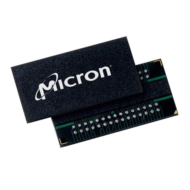
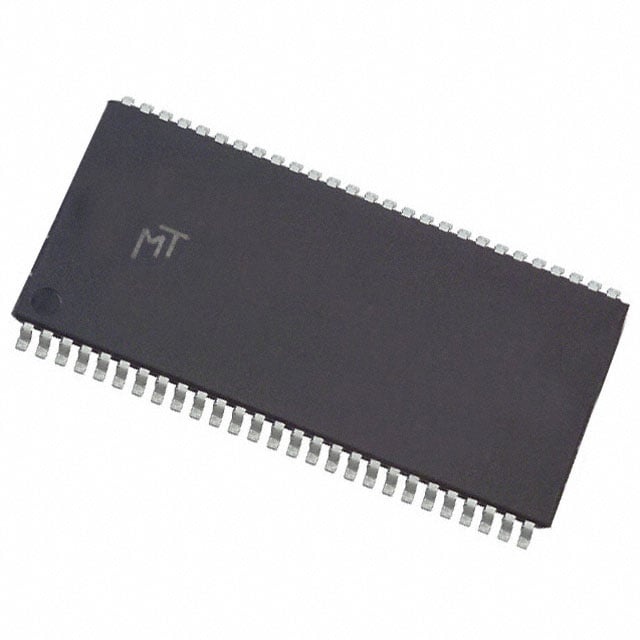
MT48LC32M8A2BB-7E:G
| Part Description |
IC DRAM 256MBIT PARALLEL 60FBGA |
|---|---|
| Quantity | 1,511 Available (as of June 15, 2026) |

| Product Category | Memory |
|---|---|
| Manufacturer | Micron Technology Inc. |
| Manufacturing Status | Obsolete |
| Manufacturer Standard Lead Time | Contact Us |
| Datasheet |
Specifications & Environmental
| Device Package | 60-FBGA (8x16) | Memory Format | DRAM | Technology | SDRAM | ||
|---|---|---|---|---|---|---|---|
| Memory Size | 256 Mbit | Access Time | 5.4 ns | Grade | Commercial | ||
| Clock Frequency | 133 MHz | Voltage | 3V ~ 3.6V | Memory Type | Volatile | ||
| Operating Temperature | 0°C ~ 70°C (TA) | Write Cycle Time Word Page | 14 ns | Packaging | 60-FBGA | ||
| Mounting Method | Volatile | Memory Interface | Parallel | Memory Organization | 32M x 8 | ||
| Moisture Sensitivity Level | 3 (168 Hours) | RoHS Compliance | ROHS3 Compliant | REACH Compliance | REACH Unaffected | ||
| Qualification | N/A | ECCN | EAR99 | HTS Code | 8542.32.0024 |
Overview of MT48LC32M8A2BB-7E:G – IC DRAM 256MBIT PARALLEL 60FBGA
The MT48LC32M8A2BB-7E:G is a 256 Mbit volatile SDRAM organized as 32M × 8 with a parallel memory interface in a 60-ball FBGA (8 × 16) package. It implements fully synchronous SDR SDRAM architecture and targets systems requiring standard SDRAM timing at a 133 MHz clock frequency.
Key value drivers include a compact FBGA footprint for high-density boards, standard PC100/PC133 timing compatibility from the datasheet feature set, and on-chip features for pipelined operation and internal bank management to optimize throughput within its specified commercial temperature range.
Key Features
- Memory core and organization — 256 Mbit SDRAM organized as 32M × 8 with four internal banks, providing standard SDR SDRAM architecture.
- Performance / Timing — Rated for a 133 MHz clock frequency (speed grade -7E) with target timing of 2-2-2 (RCD-RP-CL) per datasheet timing tables; access time listed as 5.4 ns and write cycle time (word/page) of 14 ns.
- SDR SDRAM functionality — Fully synchronous operation with internal pipelined operation, programmable burst lengths (1, 2, 4, 8, or full page), and support for auto precharge and auto refresh modes as documented in the product family datasheet.
- Supply and I/O — Single-supply operation in the 3.0 V to 3.6 V range with LVTTL-compatible inputs and outputs noted in the datasheet feature set.
- Package and mounting — 60-ball FBGA (8 mm × 16 mm) package (60-FBGA, 8×16) suitable for surface-mount, high-density board designs.
- Operating range — Commercial temperature operation specified from 0°C to 70°C (TA).
Typical Applications
- Systems requiring 256 Mbit SDRAM — Use where a 32M × 8 SDRAM device is needed for parallel memory subsystems.
- PC100 / PC133 timing platforms — Suitable for designs adhering to PC100 and PC133 timing classes referenced in the family feature set.
- High-density board designs — Compact 60-ball FBGA package supports space-constrained board layouts requiring surface-mount DRAM.
Unique Advantages
- Industry-standard SDRAM timing: Speed grade -7E targets 133 MHz with 2-2-2 timing, enabling straightforward integration with systems designed around PC100/PC133 timings.
- Flexible burst and bank architecture: Programmable burst lengths and internal banks enable column changes every clock and help hide row access/precharge latencies.
- Compact FBGA package: 60-ball FBGA (8×16) provides a small footprint for high-density designs while maintaining ball-grid interconnects for reliable mounting.
- Standard supply range: Operates from 3.0 V to 3.6 V (single-supply), matching common 3.3 V SDRAM power domains.
- Commercial temperature rating: Specified for 0°C to 70°C operation for applications within the commercial temperature range.
Why Choose IC DRAM 256MBIT PARALLEL 60FBGA?
The MT48LC32M8A2BB-7E:G provides a compact, standard SDRAM option delivering 256 Mbit capacity in a 60-FBGA package with documented PC100/PC133 timing and on-chip features for pipelined operation and banked memory management. Its combination of 32M × 8 organization, 133 MHz target clock, and single 3.0–3.6 V supply makes it suitable for designs that require a conventional SDRAM interface and footprint.
This device is appropriate for engineers specifying a family-backed SDRAM solution with available datasheet-defined timing and functional options. It is positioned for designs where a 60-ball FBGA form factor, standard SDRAM timing, and commercial temperature operation are primary requirements.
If you need pricing, availability, or to request a quote for MT48LC32M8A2BB-7E:G, submit a quote request or contact sales for assistance.