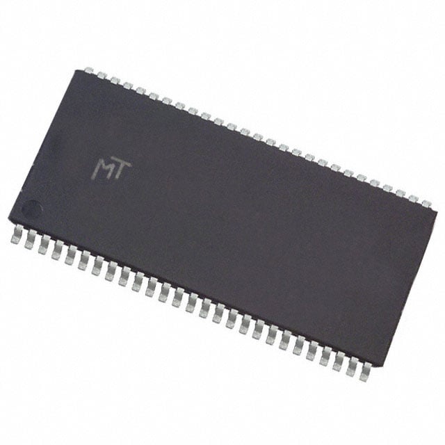
MT48LC32M8A2P-6A:D
| Part Description |
IC DRAM 256MBIT PAR 54TSOP II |
|---|---|
| Quantity | 775 Available (as of June 8, 2026) |

| Product Category | Memory |
|---|---|
| Manufacturer | Micron Technology Inc. |
| Manufacturing Status | Obsolete |
| Manufacturer Standard Lead Time | Contact Us |
| Datasheet |
Specifications & Environmental
| Device Package | 54-TSOP II | Memory Format | DRAM | Technology | SDRAM | ||
|---|---|---|---|---|---|---|---|
| Memory Size | 256 Mbit | Access Time | 5.4 ns | Grade | Commercial | ||
| Clock Frequency | 167 MHz | Voltage | 3V ~ 3.6V | Memory Type | Volatile | ||
| Operating Temperature | 0°C ~ 70°C (TA) | Write Cycle Time Word Page | 12 ns | Packaging | 54-TSOP (0.400", 10.16mm Width) | ||
| Mounting Method | Volatile | Memory Interface | Parallel | Memory Organization | 32M x 8 | ||
| Moisture Sensitivity Level | 2 (1 Year) | RoHS Compliance | ROHS3 Compliant | REACH Compliance | REACH Unaffected | ||
| Qualification | N/A | ECCN | EAR99 | HTS Code | 8542.32.0024 |
Overview of MT48LC32M8A2P-6A:D – IC DRAM 256MBIT PAR 54TSOP II
The MT48LC32M8A2P-6A:D is a 256 Mbit synchronous DRAM organized as 32M × 8 with a parallel memory interface in a 54-pin TSOP II package. It targets commercial-temperature applications requiring a fully synchronous SDRAM solution with PC100/PC133 compatibility and straightforward board-level integration.
Key characteristics include a 167 MHz clock grade, 5.4 ns access time, single 3.3 V supply range, and a 54-TSOP (400 mil / 10.16 mm width) package suited for space-constrained designs.
Key Features
- Core Architecture Fully synchronous SDRAM with internal pipelined operation and four internal banks to optimize row access and precharge handling.
- Memory Organization & Density 256 Mbit capacity organized as 32M × 8 (8 Meg × 8 × 4 banks) suitable for parallel DRAM system memory needs.
- Performance 167 MHz clock frequency (–6A speed grade) with a 5.4 ns access time and programmable CAS latency options consistent with PC100/PC133 timing.
- Timing & Burst Control Programmable burst lengths (1, 2, 4, 8, or full page), auto precharge and auto refresh modes, and support for standard refresh intervals (8192 cycles).
- Power Single 3.3 V ±0.3 V supply (3.0 V to 3.6 V) for system-level compatibility with common DRAM power domains.
- Package & Mounting 54-pin TSOP II (0.400" / 10.16 mm width) plastic package for surface-mount assembly and compact PCB layouts.
- Operating Range Commercial temperature rating of 0°C to +70°C (TA), matching standard commercial system requirements.
- Interface Parallel SDRAM interface with LVTTL-compatible inputs/outputs for direct integration into synchronous memory buses.
Typical Applications
- Commercial Embedded Systems System memory for embedded controllers and processing modules operating within commercial temperature ranges.
- Consumer Electronics Synchronous DRAM for devices requiring parallel SDRAM density and timing predictable for display or buffering tasks.
- Networking & Communications Equipment Buffer and working memory in network modules where PC100/PC133 timing compatibility and low-latency access are required.
Unique Advantages
- Verified PC100/PC133 Timing Compatibility: Designed to meet PC100 and PC133 timing profiles, easing integration into systems targeting those clock domains.
- High-Frequency Operation: 167 MHz speed grade delivers low access latency (5.4 ns) for workloads sensitive to read/write response times.
- Compact TSOP II Package: 54-pin TSOP II (400 mil / 10.16 mm) enables dense board layouts while providing standard surface-mount mounting.
- Flexible Burst and Refresh Modes: Programmable burst lengths, auto precharge, and auto refresh modes simplify memory control and improve throughput predictability.
- Single-Supply Simplicity: Operates from a single 3.3 V supply (3.0–3.6 V), simplifying power-rail design in commercial systems.
- Commercial Temperature Specification: 0°C to +70°C rating aligns with typical commercial deployments and thermal profiles.
Why Choose IC DRAM 256MBIT PAR 54TSOP II?
The MT48LC32M8A2P-6A:D offers a straightforward, fully synchronous 256 Mbit SDRAM solution tailored for commercial-temperature systems that require predictable timing, PC100/PC133 compatibility, and compact packaging. Its 32M × 8 organization, 167 MHz speed grade, and programmable burst modes make it suitable for designs where low-latency parallel memory and standard SDRAM control are priorities.
This part is appropriate for engineers and procurement teams building commercial embedded platforms, consumer devices, or networking equipment who need a verified synchronous DRAM memory device with a small-footprint TSOP II package and standard 3.3 V supply requirements.
If you would like pricing, availability, or to request a formal quote for the MT48LC32M8A2P-6A:D, please submit a quote request or inquiry to receive further assistance.