MT48LC32M8A2P-75 IT:D
| Part Description |
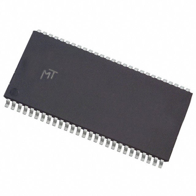
IC DRAM 256MBIT PAR 54TSOP II |
|---|---|
| Quantity | 1,675 Available (as of June 15, 2026) |

| Product Category | Memory |
|---|---|
| Manufacturer | Micron Technology Inc. |
| Manufacturing Status | Obsolete |
| Manufacturer Standard Lead Time | Contact Us |
| Datasheet |
Specifications & Environmental
| Device Package | 54-TSOP II | Memory Format | DRAM | Technology | SDRAM | ||
|---|---|---|---|---|---|---|---|
| Memory Size | 256 Mbit | Access Time | 5.4 ns | Grade | Industrial | ||
| Clock Frequency | 133 MHz | Voltage | 3V ~ 3.6V | Memory Type | Volatile | ||
| Operating Temperature | -40°C ~ 85°C (TA) | Write Cycle Time Word Page | 15 ns | Packaging | 54-TSOP (0.400", 10.16mm Width) | ||
| Mounting Method | Volatile | Memory Interface | Parallel | Memory Organization | 32M x 8 | ||
| Moisture Sensitivity Level | 2 (1 Year) | RoHS Compliance | ROHS3 Compliant | REACH Compliance | REACH Unaffected | ||
| Qualification | N/A | ECCN | EAR99 | HTS Code | 8542.32.0024 |
Overview of MT48LC32M8A2P-75 IT:D – IC DRAM 256MBIT PAR 54TSOP II
The MT48LC32M8A2P-75 IT:D is a 256 Mbit SDR SDRAM device organized as 32M × 8 with a parallel memory interface in a 54-pin TSOP II (400 mil) package. It targets applications that require synchronous DRAM with PC100/PC133 timing compliance, offering standard SDRAM features for burst transfers and internal banked operation.
This device delivers 133 MHz clock operation with a single 3.3 V ±0.3 V supply and supports industrial ambient operation from −40 °C to +85 °C, making it suitable for designs needing a compact, parallel SDRAM memory solution in a TSOP II footprint.
Key Features
- Core / Memory 256 Mbit SDR SDRAM organized as 32M × 8 with four internal banks to improve efficient row access and precharge handling.
- Performance & Timing PC100- and PC133-compliant operation with a rated clock frequency of 133 MHz and an access time of 5.4 ns; timing options include 3-3-3 and 2-2-2 CAS/RCD/RP configurations per the datasheet.
- Burst and Refresh Functions Programmable burst lengths (1, 2, 4, 8, or full page), auto precharge, auto refresh and a self-refresh mode (self-refresh not available on AT devices); supports 8192-cycle refresh.
- Interface & I/O Parallel memory interface with LVTTL-compatible inputs and outputs and fully synchronous operation where all signals are registered on the positive edge of the system clock.
- Power Single-supply operation at 3.3 V ±0.3 V (3.0 V to 3.6 V) to match standard SDRAM system rails.
- Package & Temperature 54-pin TSOP II (0.400", 10.16 mm width) plastic package; industrial operating temperature range of −40 °C to +85 °C (TA) for extended-environment deployments.
Typical Applications
- PC memory subsystems Use in systems requiring PC100/PC133-compliant SDRAM timing and standard SDRAM functionality.
- Industrial embedded systems Suitable for embedded designs that need parallel SDRAM operation across an industrial temperature range (−40 °C to +85 °C).
- Legacy and replacement designs Fits designs requiring a compact 54-pin TSOP II SDRAM package with a 32M × 8 organization and standard 3.3 V supply.
Unique Advantages
- Industry-standard timing compatibility: PC100/PC133 compliance and multiple CAS/RCD/RP timing options simplify integration into systems designed around these standards.
- Flexible burst operation: Programmable burst lengths and internal pipelined operation allow column address changes every clock cycle for efficient data throughput.
- Compact TSOP II packaging: The 54-pin TSOP II (400 mil) footprint offers a dense, board-friendly form factor for space-constrained designs.
- Industrial temperature support: Rated for −40 °C to +85 °C ambient operation, enabling use in a wider range of environmental conditions.
- Single 3.3 V supply: Standard 3.0–3.6 V supply range aligns with common SDRAM power rails for straightforward board-level power design.
Why Choose IC DRAM 256MBIT PAR 54TSOP II?
The MT48LC32M8A2P-75 IT:D provides a compact, industry-standard SDR SDRAM solution with a 32M × 8 organization and PC100/PC133 timing compatibility. Its combination of programmable burst modes, internal bank architecture and LVTTL I/O support enables predictable synchronous operation in parallel-memory designs.
This device is well suited for engineers and procurement teams specifying 256 Mbit parallel SDRAM in a 54-pin TSOP II package who require 3.3 V single-supply operation and industrial temperature capability for extended-environment applications.
Request a quote or submit a procurement inquiry for the MT48LC32M8A2P-75 IT:D to receive pricing and availability details for your design or production requirements.