
MT48LC32M8A2P-75:D
| Part Description |
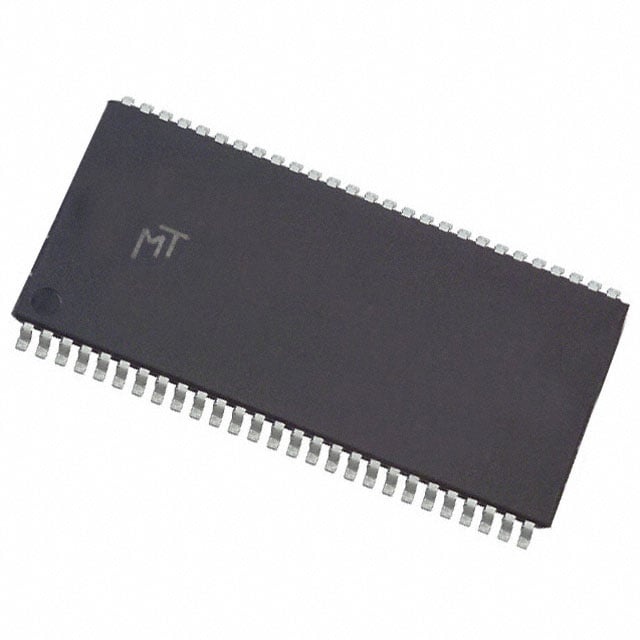
IC DRAM 256MBIT PAR 54TSOP II |
|---|---|
| Quantity | 30 Available (as of June 9, 2026) |
| Product Category | Memory |
|---|---|
| Manufacturer | Micron Technology Inc. |
| Manufacturing Status | Obsolete |
| Manufacturer Standard Lead Time | Contact Us |
| Datasheet |
Specifications & Environmental
| Device Package | 54-TSOP II | Memory Format | DRAM | Technology | SDRAM | ||
|---|---|---|---|---|---|---|---|
| Memory Size | 256 Mbit | Access Time | 5.4 ns | Grade | Commercial | ||
| Clock Frequency | 133 MHz | Voltage | 3V ~ 3.6V | Memory Type | Volatile | ||
| Operating Temperature | 0°C ~ 70°C (TA) | Write Cycle Time Word Page | 15 ns | Packaging | 54-TSOP (0.400", 10.16mm Width) | ||
| Mounting Method | Volatile | Memory Interface | Parallel | Memory Organization | 32M x 8 | ||
| Moisture Sensitivity Level | 2 (1 Year) | RoHS Compliance | ROHS Compliant | REACH Compliance | REACH Unaffected | ||
| Qualification | N/A | ECCN | EAR99 | HTS Code | 8542.32.0024 |
Overview of MT48LC32M8A2P-75:D – IC DRAM 256MBIT PAR 54TSOP II
The MT48LC32M8A2P-75:D is a 256 Mbit synchronous DRAM device organized as 32M × 8 with a parallel memory interface. It implements SDR SDRAM architecture with internal banks, programmable burst lengths and synchronous operation tied to a system clock.
Designed for commercial-temperature applications, the device targets systems that require PC100/PC133-class parallel SDRAM memory operating at up to 133 MHz with a single 3.0–3.6 V supply and a compact 54-pin TSOP II package.
Key Features
- Memory Architecture — 256 Mbit organized as 32M × 8 with 4 internal banks, providing standard DRAM organization for parallel-system designs.
- SDR SDRAM Core — Fully synchronous SDRAM; all signals are registered on the positive edge of the system clock and internal pipelining allows column-address changes every clock cycle.
- PC100 / PC133 Compliance — Device is described as PC100- and PC133-compliant with a clock frequency option at 133 MHz (speed grade -75).
- Timing and Performance — Specified clock frequency of 133 MHz and an access time listed at 5.4 ns; write cycle time (word/page) of 15 ns. CAS latency and timing targets are defined by speed grade.
- Programmable Burst & Refresh — Supports programmable burst lengths (1, 2, 4, 8, full page), auto precharge, auto refresh and self-refresh modes as documented for the family.
- Power — Single supply operation across 3.0 V to 3.6 V for standard 3.3 V systems.
- Package & Mounting — 54-pin TSOP II (0.400", 10.16 mm width) plastic package suitable for surface-mount assembly.
- Operating Range — Commercial operating temperature range of 0°C to +70°C (TA).
Typical Applications
- Embedded Systems — Provides parallel SDRAM capacity for legacy and contemporary embedded controllers requiring 256 Mbit memory in a TSOP II package.
- Networking & Communications — Suitable for buffer and working memory in network devices where PC100/PC133-class SDRAM timing and parallel interface are required.
- Consumer and Industrial Electronics — Fits designs needing synchronous DRAM with commercial temperature range and standard 3.3 V supply.
Unique Advantages
- Standard SDRAM timing and compliance: PC100/PC133-compliant operation at up to 133 MHz enables use in systems designed around those timing classes.
- Flexible burst and bank management: Programmable burst lengths and internal bank structure allow efficient row/column access patterns and higher sustained throughput for burst transfers.
- Compact surface-mount package: 54-pin TSOP II (400 mil) package offers a small-footprint solution for board-level integration.
- Single-supply compatibility: 3.0–3.6 V operation aligns with standard 3.3 V system power rails for straightforward integration.
- Commercial temperature-rated: Rated for 0°C to +70°C operation for use in typical commercial electronics environments.
Why Choose MT48LC32M8A2P-75:D?
The MT48LC32M8A2P-75:D delivers a proven SDR SDRAM architecture with 256 Mbit density, PC100/PC133-class timing, and a standard 54-pin TSOP II package for compact, board-level integration. Its synchronous operation, programmable burst lengths and internal bank architecture make it appropriate for systems that require predictable, clock-synchronous parallel memory behavior.
This device is suited to designers and procurement teams specifying commercial-temperature parallel SDRAM at 3.3 V, and it is supported by Micron documentation for timing, refresh and mode options to aid system design and validation.
Request a quote or submit an inquiry to receive pricing and availability for the MT48LC32M8A2P-75:D and to discuss volume, lead times, or qualification details.


