MT48LC4M32B2TG-7:G TR
| Part Description |
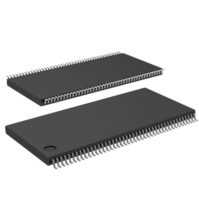
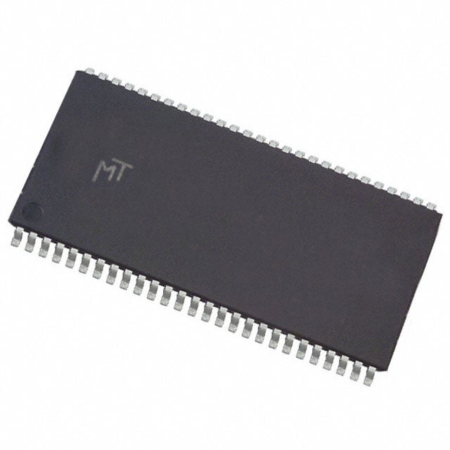
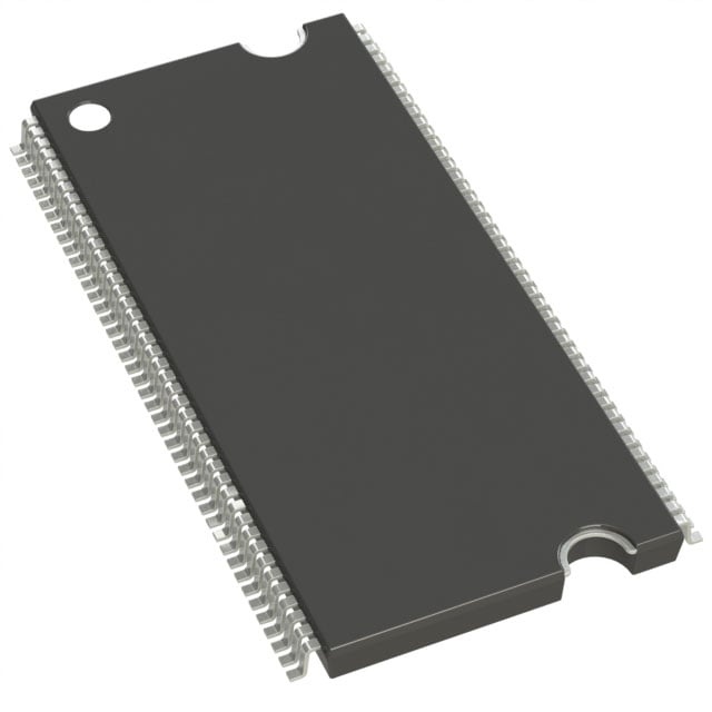
IC DRAM 128MBIT PAR 86TSOP II |
|---|---|
| Quantity | 311 Available (as of June 9, 2026) |
| Product Category | Memory |
|---|---|
| Manufacturer | Micron Technology Inc. |
| Manufacturing Status | Obsolete |
| Manufacturer Standard Lead Time | Contact Us |
| Datasheet |
Specifications & Environmental
| Device Package | 86-TSOP II | Memory Format | DRAM | Technology | SDRAM | ||
|---|---|---|---|---|---|---|---|
| Memory Size | 128 Mbit | Access Time | 5.5 ns | Grade | Commercial | ||
| Clock Frequency | 143 MHz | Voltage | 3V ~ 3.6V | Memory Type | Volatile | ||
| Operating Temperature | 0°C ~ 70°C (TA) | Write Cycle Time Word Page | 14 ns | Packaging | 86-TFSOP (0.400", 10.16mm Width) | ||
| Mounting Method | Volatile | Memory Interface | Parallel | Memory Organization | 4M x 32 | ||
| Moisture Sensitivity Level | 2 (1 Year) | RoHS Compliance | RoHS non-compliant | REACH Compliance | REACH Unaffected | ||
| Qualification | N/A | ECCN | EAR99 | HTS Code | 8542.32.0002 |
Overview of MT48LC4M32B2TG-7:G TR – IC DRAM 128MBIT PAR 86TSOP II
The MT48LC4M32B2TG-7:G TR is a 128 Mbit SDRAM device organized as 4M × 32 with a parallel memory interface. It provides synchronous DRAM storage with defined timing and voltage characteristics for systems that require straightforward parallel SDRAM integration.
Key attributes include a 143 MHz clock frequency, 5.5 ns access time, and operation from 3.0 V to 3.6 V, packaged in an 86-TSOP II (0.400", 10.16 mm width) form factor.
Key Features
- Core / Memory Architecture — 128 Mbit SDRAM organized as 4M × 32, offering parallel DRAM storage for synchronous memory designs.
- Performance — 143 MHz clock frequency with a 5.5 ns access time and a 14 ns write cycle time (word/page), providing deterministic timing for memory transactions.
- Memory Interface — Parallel memory interface compatible with parallel SDRAM bus implementations.
- Power — Operating supply voltage range of 3.0 V to 3.6 V to match common 3 V SDRAM systems.
- Package — 86-TFSOP (86-TSOP II) package with 0.400" (10.16 mm) width for board-level footprint consistency.
- Operating Temperature — Specified ambient operating range of 0°C to 70°C (TA).
Typical Applications
- Parallel SDRAM subsystems — Integration as local volatile storage where a parallel SDRAM architecture is required for synchronous burst access.
- Legacy and board-level memory upgrades — Replacement or population in designs that use an 86-TSOP II package and parallel SDRAM footprint.
- Embedded systems — Use in embedded designs that require 128 Mbit of volatile SDRAM with defined access timing and 3.0–3.6 V supply compatibility.
Unique Advantages
- Known density and organization: 4M × 32 layout provides a clear memory map for system designers working with 128 Mbit SDRAM.
- Deterministic timing: 5.5 ns access time and 14 ns write cycle time offer explicit timing parameters for predictable memory operation.
- Standard supply range: 3.0–3.6 V operation aligns with common 3 V SDRAM power rails.
- Compact TSOP II package: 86-TSOP II (0.400", 10.16 mm) footprint supports board designs targeting this package family.
- Parallel interface: Direct compatibility with parallel SDRAM buses simplifies integration into systems using parallel memory architectures.
Why Choose MT48LC4M32B2TG-7:G TR?
The MT48LC4M32B2TG-7:G TR is positioned as a straightforward 128 Mbit parallel SDRAM option with explicit timing, voltage, and package specifications. Its combination of 4M × 32 organization, 143 MHz clock capability, and defined access and write-cycle times make it suitable for designs that require predictable SDRAM behavior in an 86-TSOP II footprint.
Designers and procurement teams can use this device where 3.0–3.6 V operation, parallel interface compatibility, and the stated operating temperature range (0°C to 70°C) meet system requirements, providing a clear, spec-driven choice for volatile memory needs.
Request a quote or contact sales to submit volume pricing and lead-time information for the MT48LC4M32B2TG-7:G TR.